- 您現(xiàn)在的位置:買賣IC網(wǎng) > PDF目錄1887 > 20-101-1131 (Rabbit Semiconductor)MODULE RCM4200 RABBITCORE PDF資料下載
參數(shù)資料
| 型號(hào): | 20-101-1131 |
| 廠商: | Rabbit Semiconductor |
| 文件頁數(shù): | 78/134頁 |
| 文件大小: | 0K |
| 描述: | MODULE RCM4200 RABBITCORE |
| 產(chǎn)品培訓(xùn)模塊: | WiFi Authentication |
| 標(biāo)準(zhǔn)包裝: | 1 |
| 系列: | RabbitCore® |
| 模塊/板類型: | MPU 核心模塊 |
| 適用于相關(guān)產(chǎn)品: | RCM4200 |
| 其它名稱: | 316-1124 |
第1頁第2頁第3頁第4頁第5頁第6頁第7頁第8頁第9頁第10頁第11頁第12頁第13頁第14頁第15頁第16頁第17頁第18頁第19頁第20頁第21頁第22頁第23頁第24頁第25頁第26頁第27頁第28頁第29頁第30頁第31頁第32頁第33頁第34頁第35頁第36頁第37頁第38頁第39頁第40頁第41頁第42頁第43頁第44頁第45頁第46頁第47頁第48頁第49頁第50頁第51頁第52頁第53頁第54頁第55頁第56頁第57頁第58頁第59頁第60頁第61頁第62頁第63頁第64頁第65頁第66頁第67頁第68頁第69頁第70頁第71頁第72頁第73頁第74頁第75頁第76頁第77頁當(dāng)前第78頁第79頁第80頁第81頁第82頁第83頁第84頁第85頁第86頁第87頁第88頁第89頁第90頁第91頁第92頁第93頁第94頁第95頁第96頁第97頁第98頁第99頁第100頁第101頁第102頁第103頁第104頁第105頁第106頁第107頁第108頁第109頁第110頁第111頁第112頁第113頁第114頁第115頁第116頁第117頁第118頁第119頁第120頁第121頁第122頁第123頁第124頁第125頁第126頁第127頁第128頁第129頁第130頁第131頁第132頁第133頁第134頁
42
RabbitCore RCM4200
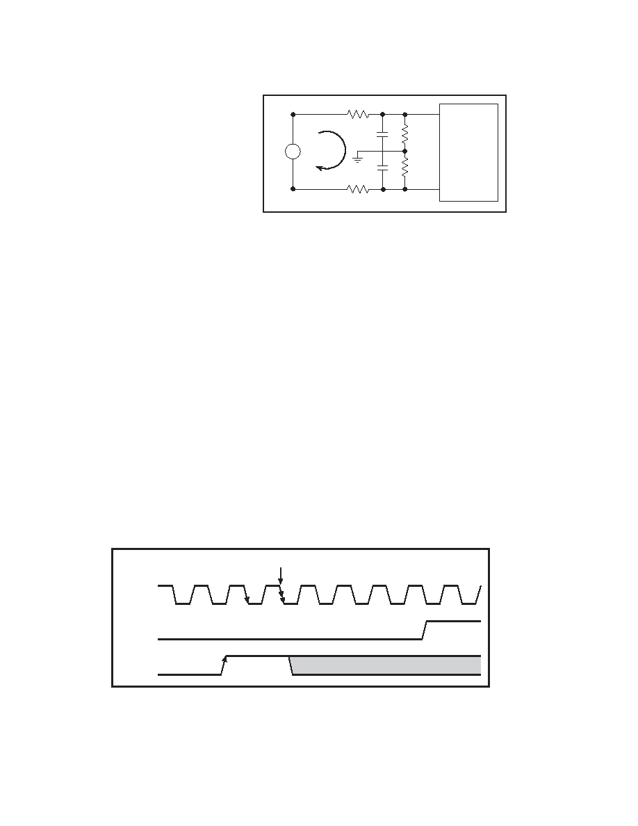
If a device such as a battery is
connected across two channels
for a differential measurement,
and it is not referenced to
analog ground, then the current
from the device will flow
through both sets of attenuator
resistors without flowing back
to analog ground as shown in
Figure 11. This will generate a
negative voltage at one of the
inputs, LN1, which will almost
certainly lead to inaccurate A/D
conversions. To make such differential measurements, connect the R1 resistors to the A/D
converter’s internal reference voltage, which is software-configurable for 1.15 V, 2.048 V,
or 2.5 V. This internal reference voltage is available on pin 49 of header J2 as VREF, and
allows you to convert analog input voltages that are negative with respect to analog ground.
NOTE: The amplifier inside the A/D converter’s internal voltage reference circuit has a
very limited output-current capability. The internal buffer can source up to 20 mA and
sink only up to 200 A. Use a separate buffer amplifier if you need to supply any load
current.
The A/D converter’s CONVERT pin is available on pin 48 of header J2 and can be used as
a hardware means of forcing the A/D converter to start a conversion cycle at a specific time.
The CONVERT signal is an edge-triggered event and has a hold time of two CCLK periods
for debounce.
A conversion is started by an active (rising) edge on the CONVERT pin. The CONVERT
pin must stay low for at least two CCLK periods before going high for at least two CCLK
periods. Figure 12 shows the timing of a conversion start. The double falling arrow on
CCLK indicates the actual start of the conversion cycle.
Figure 12. Timing Diagram for Conversion Start Using CONVERT Pin
Appendix B explains the implementation examples of these features on the Prototyping
Board.
Figure 11. Current Flow from Ungrounded
or Floating Source
R0
2.2 nF
R1
2.2 nF
ADC
AIN0
AIN1
+
I
LN0
LN1
+
-
Device
CCLK
BUSY
CONV
Conversion starts
相關(guān)PDF資料 |
PDF描述 |
|---|---|
| 20-101-1139 | RCM4310 RABBITCORE |
| 20-101-1154 | MODULE RCM4120 RABBITCORE |
| 20-101-1197 | MODULE RABBITCORE RCM3910 ROHS |
| 20-101-1215 | MCU RCM4050 RABBITCORE |
| 20-101-1246 | CORE MODULE RCM5400W |
相關(guān)代理商/技術(shù)參數(shù) |
參數(shù)描述 |
|---|---|
| 20-101-1132 | 功能描述:模塊化系統(tǒng) - SOM RCM4210 RabbitCore- Module RoHS:否 制造商:Digi International 外觀尺寸:ConnectCore 9P 處理器類型:ARM926EJ-S 頻率:150 MHz 存儲(chǔ)容量:8 MB, 16 MB 存儲(chǔ)類型:NOR Flash, SDRAM 接口類型:I2C, SPI, UART 工作電源電壓:3.3 V 最大工作溫度:+ 85 C 尺寸:1.97 in x 1.97 in x 6.1 in |
| 20-101-1136 | 功能描述:射頻模塊 RF Module Interface RoHS:否 制造商:Linx Technologies 產(chǎn)品:Transceiver Modules 頻帶:902 MHz to 928 MHz 輸出功率:- 15.5 dBm to + 12.5 dBm 接口類型:UART 工作電源電壓:- 0.3 VDC to + 5.5 VDC 傳輸供電電流:38.1 mA 接收供電電流:22.7 mA 天線連接器類型:U.FL 最大工作溫度:+ 85 C 尺寸:1.15 mm x 0.63 mm x 0.131 mm |
| 20-101-1138 | 功能描述:模塊化系統(tǒng) - SOM RCM4300 RABBITCORE RoHS:否 制造商:Digi International 外觀尺寸:ConnectCore 9P 處理器類型:ARM926EJ-S 頻率:150 MHz 存儲(chǔ)容量:8 MB, 16 MB 存儲(chǔ)類型:NOR Flash, SDRAM 接口類型:I2C, SPI, UART 工作電源電壓:3.3 V 最大工作溫度:+ 85 C 尺寸:1.97 in x 1.97 in x 6.1 in |
| 20-101-1139 | 功能描述:模塊化系統(tǒng) - SOM RCM4310 RABBITCORE RoHS:否 制造商:Digi International 外觀尺寸:ConnectCore 9P 處理器類型:ARM926EJ-S 頻率:150 MHz 存儲(chǔ)容量:8 MB, 16 MB 存儲(chǔ)類型:NOR Flash, SDRAM 接口類型:I2C, SPI, UART 工作電源電壓:3.3 V 最大工作溫度:+ 85 C 尺寸:1.97 in x 1.97 in x 6.1 in |
| 20-101-1140 | 功能描述:WiFi/802.11模塊 RCM4400W CORE MODULE Wi-Fi/802.11 RoHS:否 制造商:Taiyo Yuden 支持協(xié)議:802.11 b/g/n 頻帶: 數(shù)據(jù)速率:150 Mbps 接口類型:SDIO 傳輸功率(最大): 天線連接器類型: 工作電源電壓:3.4 V to 5.5 V 傳輸供電電流: 接收供電電流: 最大工作溫度:+ 80 C 尺寸:35 mm x 15 mm x 2.9 mm |
發(fā)布緊急采購,3分鐘左右您將得到回復(fù)。