- 您現(xiàn)在的位置:買賣IC網(wǎng) > PDF目錄9084 > XRT71D04IVTR (Exar Corporation)IC JITTER ATTENUATOR 4CH 80TQFP PDF資料下載
參數(shù)資料
| 型號(hào): | XRT71D04IVTR |
| 廠商: | Exar Corporation |
| 文件頁(yè)數(shù): | 19/22頁(yè) |
| 文件大?。?/td> | 0K |
| 描述: | IC JITTER ATTENUATOR 4CH 80TQFP |
| 標(biāo)準(zhǔn)包裝: | 1,000 |
| 類型: | * |
| PLL: | 是 |
| 輸入: | 時(shí)鐘 |
| 輸出: | 時(shí)鐘 |
| 電路數(shù): | 1 |
| 比率 - 輸入:輸出: | 4:3 |
| 差分 - 輸入:輸出: | 無(wú)/無(wú) |
| 頻率 - 最大: | 44.736MHz |
| 除法器/乘法器: | 無(wú)/無(wú) |
| 電源電壓: | 3.135 V ~ 5.25 V |
| 工作溫度: | -40°C ~ 85°C |
| 安裝類型: | 表面貼裝 |
| 封裝/外殼: | 80-LQFP |
| 供應(yīng)商設(shè)備封裝: | 80-TQFP(14x14) |
| 包裝: | 帶卷 (TR) |
第1頁(yè)第2頁(yè)第3頁(yè)第4頁(yè)第5頁(yè)第6頁(yè)第7頁(yè)第8頁(yè)第9頁(yè)第10頁(yè)第11頁(yè)第12頁(yè)第13頁(yè)第14頁(yè)第15頁(yè)第16頁(yè)第17頁(yè)第18頁(yè)當(dāng)前第19頁(yè)第20頁(yè)第21頁(yè)第22頁(yè)
XRT71D04
á
4 CHANNEL E3/DS3/STS-1 JITTER ATTENUATOR, STS-1 TO DS3 DESYNCHRONIZER
REV. 1.1.1
5
23
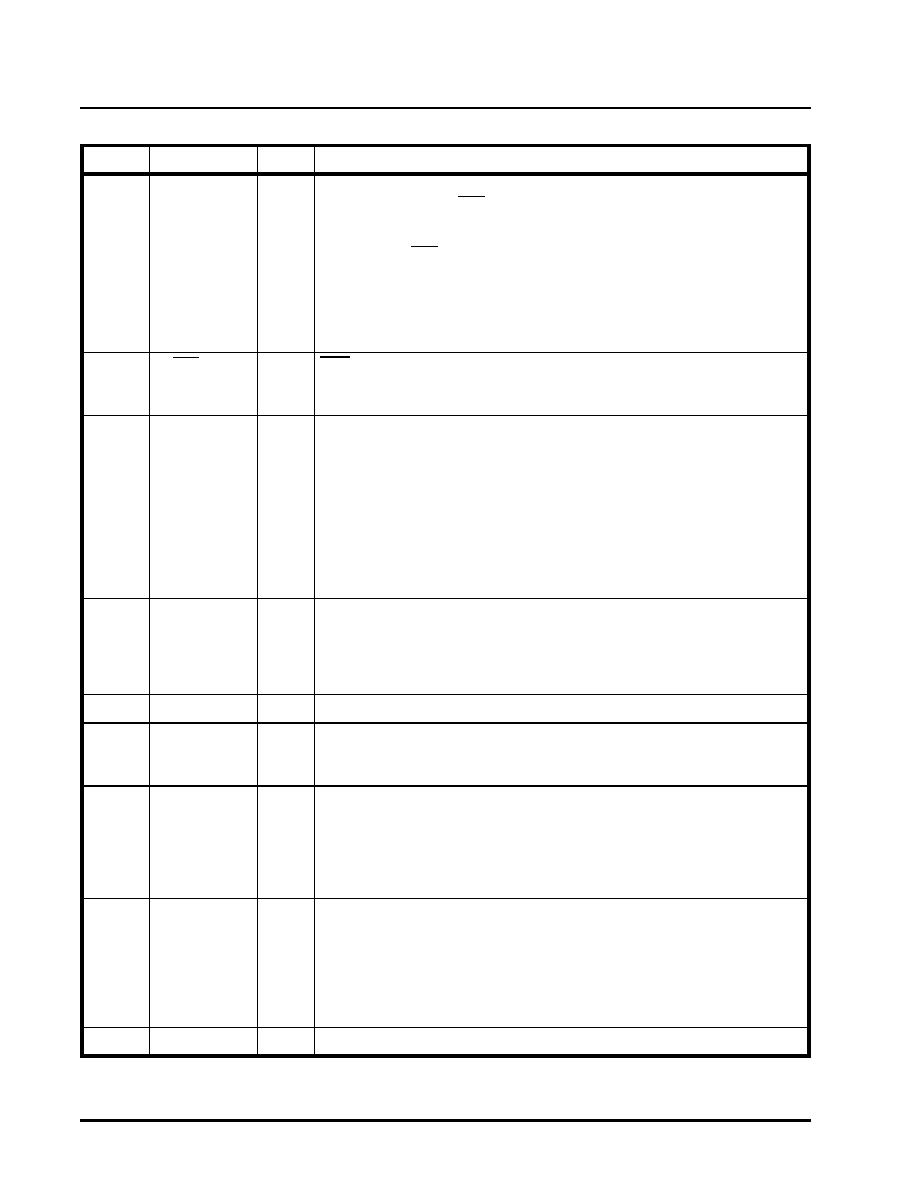
STS1_0
I
SONET STS1 Mode Select - channel 0:
This pin along with the DS3/E3_0 select pin configures the XRT71D04 either in
E3, DS3 or STS-1 mode.
A table relating to the setting of the pins is given below:
STS-1
DS3/E3
XRT71D04 Operating Mode
0
DS3 (44.736 MHz)
0
1
E3 (34.368 MHz)
1
0
STS-1 (51.84 MHz)
1
E3 (34.368 MHz)
This input pin is active only in the Hardware Mode.
24
DS3/E3_0
I
DS3/E3 Select Input - channel 0:
See description pin 10.
Internal 50 K Ohm pull-down resistor.
25
DJA_0/SCLK
I
Harware Mode
Disable Jitter Attenuator Input - Channel 0:
An active-high disables the Jitter Attenuator. The RPOS/RNEG and RCLK will be
passed through without jitter attenuation.
Host Mode
Microprocessor Serial Interface Clock Signal:
This signal will be used to (1) sample the data, on the SDI pin, on the rising edge
of this signal. Additionally, during “Read” operations, the Microprocessor Serial
Interface will update the SDO output on the falling edge of this signal.
Internal 50 K Ohm pull-down resistor.
26
MCLK_3
I
Master Clock Input - channel 3:
Reference clock for internal PLL. 44.736MHz+/-20ppm or 34.368MHz+/-20ppm.
This clock must be continuous and jitter free with duty cycle between 30 to 70%.
It is permissible to use the EXCLK signal orSTS1 clock.
Internal 50 K Ohm pull-up resistor.
27
GND
****
Digital Ground
28
RCLK_3
I
Received Clock (Jittery) - channel 3:
Clock input RCLK3 should be connected to the recovered clock.
Internal 50 K Ohm pull-up resistor.
29
RPOS_2
I
Received Positive Data (Jittery) Input: - channel 2:
Data that is input on this pin is sampled on either the rising or falling edge of
RCLK depending on the setting of the RCLKES pin (pin 10).
If RCLKES is “high”, then RPOS will be sampled on the falling edge of RCLK.
If RCLKES is “l(fā)ow”, then RPOS will be sampled on the rising edge of RCLK.
Internal 50 K Ohm pull-up resistor.
30
RNEG_2
I
Received Negative Data (Jittery) - channel 2:
The input jittery negative data is sampled either on the rising or falling edge of
RCLK depending on the setting of RCLKES.
If RCLKES is “high”, then RNEG will be sampled on the falling edge of RCLK.
If RCLKES is “l(fā)ow”, then RPOS will be sampled on the rising edge of RCLK.
This pin is typically tied to the “RNEG” output pin of the LIU.
Internal 50 K Ohm pull-up resistor.
31
VDD
****
Digital Power Supply = 5V±5% or 3.3V±5%
PIN DESCRIPTION
PIN #NAME
TYPE
DESCRIPTION
相關(guān)PDF資料 |
PDF描述 |
|---|---|
| VI-2T1-MW-S | CONVERTER MOD DC/DC 12V 100W |
| MS27474T24F29S | CONN RCPT 29POS JAM NUT W/SCKT |
| V28A6V5H200BF2 | CONVERTER MOD DC/DC 6.5V 200W |
| V28A6V5H200B2 | CONVERTER MOD DC/DC 6.5V 200W |
| XRT71D03IVTR-F | IC JITTER ATTENUATOR 3CH 64TQFP |
相關(guān)代理商/技術(shù)參數(shù) |
參數(shù)描述 |
|---|---|
| XRT7250 | 制造商:EXAR 制造商全稱:EXAR 功能描述:DS3/E3 FRAMER IC |
| XRT7250ES-PCI | 功能描述:界面開發(fā)工具 Evaluation Board for XRT7250 Series RoHS:否 制造商:Bourns 產(chǎn)品:Evaluation Boards 類型:RS-485 工具用于評(píng)估:ADM3485E 接口類型:RS-485 工作電源電壓:3.3 V |
| XRT7250IQ100 | 制造商:EXAR 制造商全稱:EXAR 功能描述:DS3/E3 FRAMER IC |
| XRT7288 | 制造商:EXAR 制造商全稱:EXAR 功能描述:CEPT1 Line Interface |
| XR-T7288 | 制造商:EXAR 制造商全稱:EXAR 功能描述:CEPT1 Line Interface |
發(fā)布緊急采購(gòu),3分鐘左右您將得到回復(fù)。