- 您現(xiàn)在的位置:買賣IC網(wǎng) > PDF目錄9084 > XRT71D00IQTR-F (Exar Corporation)IC JITTER ATTENUATOR SGL 32TQFP PDF資料下載
參數(shù)資料
| 型號: | XRT71D00IQTR-F |
| 廠商: | Exar Corporation |
| 文件頁數(shù): | 25/26頁 |
| 文件大?。?/td> | 0K |
| 描述: | IC JITTER ATTENUATOR SGL 32TQFP |
| 標準包裝: | 1,500 |
| 類型: | * |
| PLL: | 是 |
| 輸入: | 時鐘 |
| 輸出: | 時鐘 |
| 電路數(shù): | 1 |
| 比率 - 輸入:輸出: | 3:2 |
| 差分 - 輸入:輸出: | 無/無 |
| 頻率 - 最大: | 44.736MHz |
| 除法器/乘法器: | 無/無 |
| 電源電壓: | 3.135 V ~ 5.25 V |
| 工作溫度: | -40°C ~ 85°C |
| 安裝類型: | 表面貼裝 |
| 封裝/外殼: | 32-LQFP |
| 供應商設備封裝: | 32-TQFP(7x7) |
| 包裝: | 帶卷 (TR) |
XRT71D00
á
E3/DS3/STS-1 JITTER ATTENUATOR
REV. 1.2.0
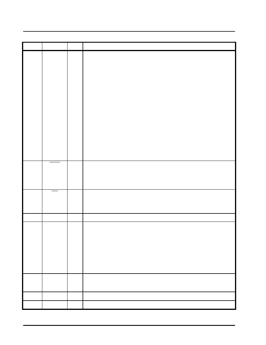
7
18
DJA/
(SDO)
I/(O)
Disable Jitter Attenuator Input/Serial Data Output pin:
The function of this pin depends on whether XRT71D00 is configured in Host or Hard-
ware mode.
Hardware Mode—Disable Jitter Attenuator:
This input pin permits the user to enable or disable the Jitter Attenuator function within
the XRT71D00 device.
Setting this input pin “high” disables the jitter attenuator PLL. Whenever the Jitter
Attenuator PLL is disabled, the the signals/data which are applied to the “RPOS”,
“RNEG” and “RCLK” input pins will pass through to the “RRPOS”, “RRNEG” and
“RRCLK” output pins without any jitter attenuation.
Setting this input pin “l(fā)ow” enables the Jitter Attenuator” PLL. Whenever the Jitter
Attenuator PLL is enabled then the signals/data which are applied to the “RPOS”,
“RNEG” and “RCLK” output pins will be routed to the “Narrow-band” PLL for jitter
reduction. The outputs of the narrow-band PLL will be routed to the “RRPOS”,
“RRNEG” and “RRCLK” output pins.
Host Mode—Serial Data Output:
This pin will serially output the contents of the specified Command Register, during
“Read” Operations. The data, on this pin, will be updated on the falling edge of the SClk
input signal. This pin will be tri-stated upon completion of data transfer.
19
Reset
I
Reset Input. (Active-Low)
A high-to-low transition will re-center and clear the contents of the internal FIFO, and
will clear the contents of the Command Registers (for Host Mode operation). Resetting
this pin may corrupt data within the device.
NOTE: For normal operation, this pin should be pulled “HIGH”.
20
ICT
I
In Circuit Testing Input. Active low.
With this pin tied to ground, all output pins will be in high impedance mode for in-circuit-
testing.
NOTE: For normal operation this input pin should be pulled “HIGH”.
21
GND
***
Digital Ground:
22
RRClk
O
Receive Output (De-jittered) Clock.
This pin outputs the “smoothed” (e.g., de-jittered) 34.368MHz, 44.736MHz or
51.84MHz clock signal. Further, this clock signal is also used to clock out the contents
of the “Recovered” data (via the “RRPOS” and “RRNEG” output pins).
If the “CLKES” pin (or bit-field) is “l(fā)ow”, then the XRT71D00 device will output data, via
the “RRPOS” and “RRNEG” output pins, upon the falling edge of this clock signal.
If the “CLKES” pin (or bit-field) is “high”, then the XRT71D00 device will output data, via
the “RRPOS” and “RRNEG” output pins, upon the rising edge of this clock signal.
23
RRNEG
O
Receive Negative Data (De-Jittered) Output.
Data which is input via the “RNEG” input pin will be updated on the rising or falling
edge of RRClk, depending upon the state of the ClkES input pin (or bit-field setting).
24
NC
***
This pin is not connected internally.
25
NC
***
This pin is not connected internally.
PIN DESCRIPTION
PIN #NAME
TYPE
DESCRIPTION
相關PDF資料 |
PDF描述 |
|---|---|
| X9421WV14I-2.7T1 | IC XDCP SGL 64-TAP 10K 14-TSSOP |
| X9421WV14-2.7T1 | IC XDCP SGL 64-TAP 10K 14-TSSOP |
| SY89536LHZ | IC SYNTHESIZR LVPECL/HSTL 64TQFP |
| VI-253-MW-S | CONVERTER MOD DC/DC 24V 100W |
| V28A5H175B | CONVERTER MOD DC/DC 5V 175W |
相關代理商/技術參數(shù) |
參數(shù)描述 |
|---|---|
| XRT71D03 | 制造商:EXAR 制造商全稱:EXAR 功能描述:3 CHANNEL E3/DS3/STS-1 JITTER ATTENUATOR |
| XRT71D03ES | 功能描述:時鐘合成器/抖動清除器 3CH T3/E3JA w/T73LC03A RoHS:否 制造商:Skyworks Solutions, Inc. 輸出端數(shù)量: 輸出電平: 最大輸出頻率: 輸入電平: 最大輸入頻率:6.1 GHz 電源電壓-最大:3.3 V 電源電壓-最小:2.7 V 封裝 / 箱體:TSSOP-28 封裝:Reel |
| XRT71D03IV | 制造商:EXAR 制造商全稱:EXAR 功能描述:3 CHANNEL E3/DS3/STS-1 JITTER ATTENUATOR |
| XRT71D03IV-F | 功能描述:時鐘合成器/抖動清除器 RoHS:否 制造商:Skyworks Solutions, Inc. 輸出端數(shù)量: 輸出電平: 最大輸出頻率: 輸入電平: 最大輸入頻率:6.1 GHz 電源電壓-最大:3.3 V 電源電壓-最小:2.7 V 封裝 / 箱體:TSSOP-28 封裝:Reel |
| XRT71D03IVTR-F | 功能描述:時鐘合成器/抖動清除器 RoHS:否 制造商:Skyworks Solutions, Inc. 輸出端數(shù)量: 輸出電平: 最大輸出頻率: 輸入電平: 最大輸入頻率:6.1 GHz 電源電壓-最大:3.3 V 電源電壓-最小:2.7 V 封裝 / 箱體:TSSOP-28 封裝:Reel |
發(fā)布緊急采購,3分鐘左右您將得到回復。