- 您現(xiàn)在的位置:買賣IC網(wǎng) > PDF目錄1975 > XR17V258IV-F (Exar Corporation)IC UART PCI BUS OCTAL 144LQFP PDF資料下載
參數(shù)資料
| 型號(hào): | XR17V258IV-F |
| 廠商: | Exar Corporation |
| 文件頁數(shù): | 57/69頁 |
| 文件大小: | 0K |
| 描述: | IC UART PCI BUS OCTAL 144LQFP |
| 標(biāo)準(zhǔn)包裝: | 60 |
| 特點(diǎn): | * |
| 通道數(shù): | 8 |
| FIFO's: | 64 字節(jié) |
| 規(guī)程: | RS485 |
| 電源電壓: | 3.3V,5V |
| 帶自動(dòng)流量控制功能: | 是 |
| 帶IrDA 編碼器/解碼器: | 是 |
| 帶故障啟動(dòng)位檢測(cè)功能: | 是 |
| 帶調(diào)制解調(diào)器控制功能: | 是 |
| 安裝類型: | 表面貼裝 |
| 封裝/外殼: | 144-LQFP |
| 供應(yīng)商設(shè)備封裝: | 144-LQFP(20x20) |
| 包裝: | 托盤 |
| 其它名稱: | 1016-1470 XR17V258IV-F-ND |
第1頁第2頁第3頁第4頁第5頁第6頁第7頁第8頁第9頁第10頁第11頁第12頁第13頁第14頁第15頁第16頁第17頁第18頁第19頁第20頁第21頁第22頁第23頁第24頁第25頁第26頁第27頁第28頁第29頁第30頁第31頁第32頁第33頁第34頁第35頁第36頁第37頁第38頁第39頁第40頁第41頁第42頁第43頁第44頁第45頁第46頁第47頁第48頁第49頁第50頁第51頁第52頁第53頁第54頁第55頁第56頁當(dāng)前第57頁第58頁第59頁第60頁第61頁第62頁第63頁第64頁第65頁第66頁第67頁第68頁第69頁
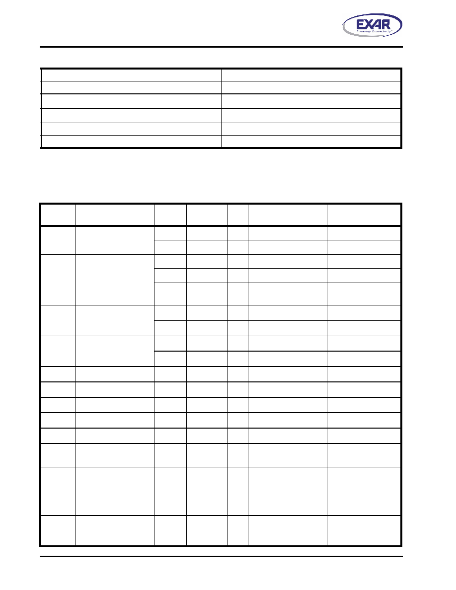
ABSOLUTE MAXIMUM RATINGS
Power Supply Range
4 Volts
Voltage at Any Pin
-0.5 to 4V
Operating Temperature
-40o to +85o C
Storage Temperature
-65o to +150C
Package Dissipation
500 mW
Thermal Resistance (20x20x1.4mm 144-LQFP)
theta-ja = 42, theta-jc = 8
ELECTRICAL CHARACTERISTICS
DC ELECTRICAL CHARACTERISTICS FOR 3.3V SIGNALLING
O TO
OC (INDUSTRIAL GRADE) SUPPLY VOLTAGE, VCC = 3.0 - 3.6V
SYMBOL
PARAMETER
MIN
MAX
UNIT
S
CONDITION
NOTES
VIL
Input Low Voltage
-0.5
0.3VCC
V
For PCI bus inputs
-0.5
0.8
V
For Non-PCI bus inputs
VIH
Input High Voltage
0.5VCC
VCC + 0.5
V
For PCI bus inputs
2.0
6.0
V
For Non-PCI bus inputs
5V tolerant inputs
2.0
VCC + 0.5
For external clock
(XTAL1) input only
Not 5V tolerant
VOL
Output Low Voltage
0.1VCC
V
IOL = 1.5mA
PCI bus outputs
0.4
V
IOL = 6mA
Non-PCI bus outputs
VOH
Output High Voltage
0.9VCC
V
IOH = -0.5mA
PCI bus outputs
2.4
V
IOH = -2mA
Non-PCI bus outputs
IIL
Input Leakage Current
±10
A
0 < Vin < VCC
ICL
Input Clock Leakage
±10
A
CIN
Input Pin Capacitance
10
pF
CCLK
CLK Pin Capacitance
5
12
pF
CIDSEL
IDSEL Pin Capacitance
8
pF
IOff
PME# input leakage
-
1
A
Vo ≤ 3.6V, VCC off or
floating
ICC
Power Supply Current
4
mA
PCI bus CLK and Ext.
Clock = 2MHz,
all inputs at VCC or
GND and all outputs are
unloaded.
ISLEEP
Sleep Current
1
mA
All eight UARTs asleep.
AD[31:0] at GND, all
inputs at VCC or GND.
XR17V258
60
66MHZ PCI BUS OCTAL UART WITH POWER MANAGEMENT SUPPORT
REV. 1.0.2
TA=-40
+85
相關(guān)PDF資料 |
PDF描述 |
|---|---|
| XR17V352IB113-F | IC UART PCIE 256B DUAL 113FPBGA |
| XR17V354IB176-F | IC UART PCIE 256B QUAD 176FPBGA |
| XR17V358IB176-F | IC UART PCIE OCTAL 176FPBGA |
| XR19L200IL32-F | IC UART/TXRX RS232 32QFN |
| XR19L202IL48-F | IC UART/TXRX RS232 48QFN |
相關(guān)代理商/技術(shù)參數(shù) |
參數(shù)描述 |
|---|---|
| XR17V258IVTR-F | 功能描述:UART 接口集成電路 66MHz Octal PCI UART RoHS:否 制造商:Texas Instruments 通道數(shù)量:2 數(shù)據(jù)速率:3 Mbps 電源電壓-最大:3.6 V 電源電壓-最小:2.7 V 電源電流:20 mA 最大工作溫度:+ 85 C 最小工作溫度:- 40 C 封裝 / 箱體:LQFP-48 封裝:Reel |
| XR17V352 | 制造商:EXAR 制造商全稱:EXAR 功能描述:HIGH PERFORMANCE DUAL PCI EXPRESS UART |
| XR17V352IB-0A-EVB | 功能描述:界面開發(fā)工具 Eval Board for XR17V352IB Series RoHS:否 制造商:Bourns 產(chǎn)品:Evaluation Boards 類型:RS-485 工具用于評(píng)估:ADM3485E 接口類型:RS-485 工作電源電壓:3.3 V |
| XR17V352IB113-F | 功能描述:UART 接口集成電路 2 Channel PCIe UART w/256 Byte FIFO RoHS:否 制造商:Texas Instruments 通道數(shù)量:2 數(shù)據(jù)速率:3 Mbps 電源電壓-最大:3.6 V 電源電壓-最小:2.7 V 電源電流:20 mA 最大工作溫度:+ 85 C 最小工作溫度:- 40 C 封裝 / 箱體:LQFP-48 封裝:Reel |
| XR17V354 | 制造商:EXAR 制造商全稱:EXAR 功能描述:HIGH PERFORMANCE QUAD PCI-EXPRESS UART |
發(fā)布緊急采購(gòu),3分鐘左右您將得到回復(fù)。