- 您現(xiàn)在的位置:買賣IC網(wǎng) > PDF目錄375033 > XCV812E-7BG900C (Xilinx, Inc.) Virtex-E 1.8 V Extended Memory Field Programmable Gate Arrays PDF資料下載
參數(shù)資料
| 型號(hào): | XCV812E-7BG900C |
| 廠商: | Xilinx, Inc. |
| 英文描述: | Virtex-E 1.8 V Extended Memory Field Programmable Gate Arrays |
| 中文描述: | 的Virtex娥內(nèi)存擴(kuò)展1.8伏現(xiàn)場(chǎng)可編程門陣列 |
| 文件頁(yè)數(shù): | 38/116頁(yè) |
| 文件大?。?/td> | 1087K |
| 代理商: | XCV812E-7BG900C |
第1頁(yè)第2頁(yè)第3頁(yè)第4頁(yè)第5頁(yè)第6頁(yè)第7頁(yè)第8頁(yè)第9頁(yè)第10頁(yè)第11頁(yè)第12頁(yè)第13頁(yè)第14頁(yè)第15頁(yè)第16頁(yè)第17頁(yè)第18頁(yè)第19頁(yè)第20頁(yè)第21頁(yè)第22頁(yè)第23頁(yè)第24頁(yè)第25頁(yè)第26頁(yè)第27頁(yè)第28頁(yè)第29頁(yè)第30頁(yè)第31頁(yè)第32頁(yè)第33頁(yè)第34頁(yè)第35頁(yè)第36頁(yè)第37頁(yè)當(dāng)前第38頁(yè)第39頁(yè)第40頁(yè)第41頁(yè)第42頁(yè)第43頁(yè)第44頁(yè)第45頁(yè)第46頁(yè)第47頁(yè)第48頁(yè)第49頁(yè)第50頁(yè)第51頁(yè)第52頁(yè)第53頁(yè)第54頁(yè)第55頁(yè)第56頁(yè)第57頁(yè)第58頁(yè)第59頁(yè)第60頁(yè)第61頁(yè)第62頁(yè)第63頁(yè)第64頁(yè)第65頁(yè)第66頁(yè)第67頁(yè)第68頁(yè)第69頁(yè)第70頁(yè)第71頁(yè)第72頁(yè)第73頁(yè)第74頁(yè)第75頁(yè)第76頁(yè)第77頁(yè)第78頁(yè)第79頁(yè)第80頁(yè)第81頁(yè)第82頁(yè)第83頁(yè)第84頁(yè)第85頁(yè)第86頁(yè)第87頁(yè)第88頁(yè)第89頁(yè)第90頁(yè)第91頁(yè)第92頁(yè)第93頁(yè)第94頁(yè)第95頁(yè)第96頁(yè)第97頁(yè)第98頁(yè)第99頁(yè)第100頁(yè)第101頁(yè)第102頁(yè)第103頁(yè)第104頁(yè)第105頁(yè)第106頁(yè)第107頁(yè)第108頁(yè)第109頁(yè)第110頁(yè)第111頁(yè)第112頁(yè)第113頁(yè)第114頁(yè)第115頁(yè)第116頁(yè)
Virtex-E 1.8 V Extended Memory Field Programmable Gate Arrays
Module 2 of 4
34
www.xilinx.com
1-800-255-7778
DS025-2 (v2.1) July 17, 2002
R
As an added convenience, the BUFGP can be used to
instantiate a high fanout clock input. The BUFGP symbol
represents a combination of the LVTTL IBUFG and BUFG
symbols, such that the output of the BUFGP can connect
directly to the clock pins throughout the design.
Unlike previous architectures, the Virtex-E BUFGP symbol
can only be placed in a global clock pad location. The LOC
property can specify a location for the BUFGP.
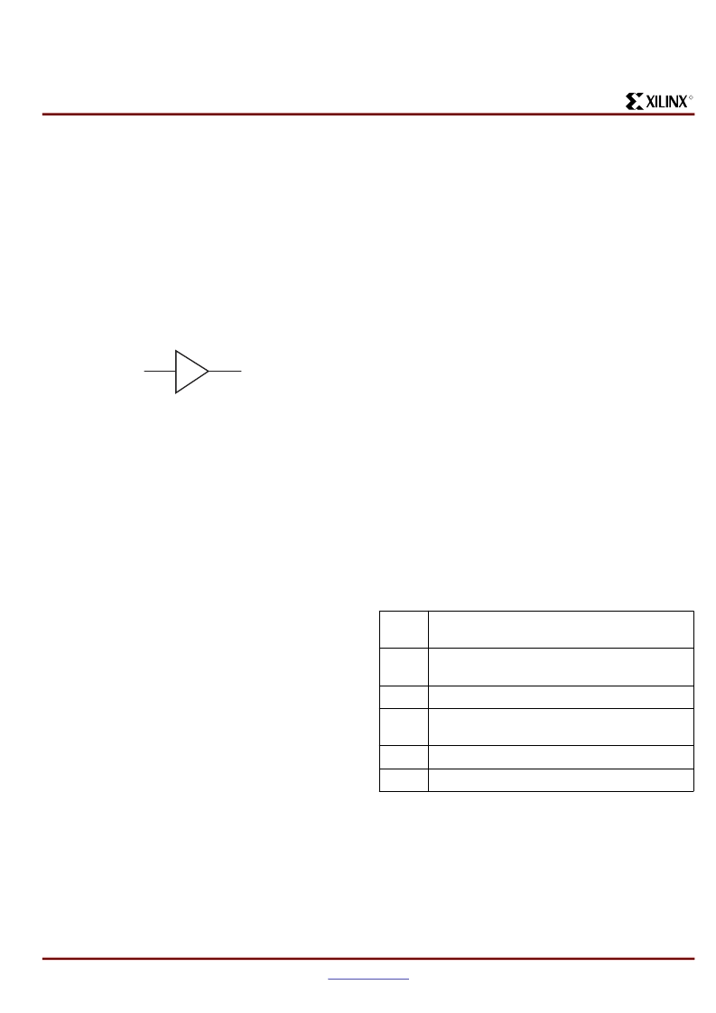
OBUF
An OBUF must drive outputs through an external output
port. The generic output buffer (OBUF) symbol appears in
Figure 40
.
The extension to the base name defines which I/O standard
the OBUF uses. With no extension specified for the generic
OBUF symbol, the assumed standard is slew rate limited
LVTTL with 12 mA drive strength.
The LVTTL OBUF additionally can support one of two slew
rate modes to minimize bus transients. By default, the slew
rate for each output buffer is reduced to minimize power bus
transients when switching non-critical signals.
LVTTL output buffers have selectable drive strengths.
The format for LVTTL OBUF symbol names is as follows.
OBUF_<slew_rate>_<drive_strength>
<slew_rate> is either F (Fast), or S (Slow) and
<drive_strength> is specified in milliamps (2, 4, 6, 8, 12, 16,
or 24).
The following list details variations of the OBUF symbol.
OBUF
OBUF_S_2
OBUF_S_4
OBUF_S_6
OBUF_S_8
OBUF_S_12
OBUF_S_16
OBUF_S_24
OBUF_F_2
OBUF_F_4
OBUF_F_6
OBUF_F_8
OBUF_F_12
OBUF_F_16
OBUF_F_24
OBUF_LVCMOS2
OBUF_PCI33_3
OBUF_PCI66_3
OBUF_GTL
OBUF_GTLP
OBUF_HSTL_I
OBUF_HSTL_III
OBUF_HSTL_IV
OBUF_SSTL3_I
OBUF_SSTL3_II
OBUF_SSTL2_I
OBUF_SSTL2_II
OBUF_CTT
OBUF_AGP
OBUF_LVCMOS18
OBUF_LVDS
OBUF_LVPECL
The Virtex-E series supports eight banks for the HQ and PQ
packages. The CS packages support four V
CCO
banks.
OBUF placement restrictions require that within a given
V
CCO
bank each OBUF share the same output source drive
voltage. Input buffers of any type and output buffers that do
not require V
CCO
can be placed within any V
CCO
bank.
Table 20
summarizes the Virtex-E output compatibility
requirements. The LOC property can specify a location for
the OBUF.
OBUFT
The generic 3-state output buffer OBUFT, shown in
Figure 41
, typically implements 3-state outputs or bidirec-
tional I/O.
The extension to the base name defines which I/O standard
OBUFT uses. With no extension specified for the generic
OBUFT symbol, the assumed standard is slew rate limited
LVTTL with 12 mA drive strength.
Figure 40:
Virtex-E Output Buffer (OBUF) Symbol
O
I
OBUF
x133_04_111699
Table 20:
Output Standards Compatibility
Requirements
Rule 1
Only outputs with standards that share compatible
V
CCO
can be used within the same bank.
Rule 2
There are no placement restrictions for outputs
with standards that do not require a V
CCO
.
V
CCO
Compatible Standards
3.3
LVTTL, SSTL3_I, SSTL3_II, CTT, AGP, GTL,
GTL+, PCI33_3, PCI66_3
2.5
SSTL2_I, SSTL2_II, LVCMOS2, GTL, GTL+
1.5
HSTL_I, HSTL_III, HSTL_IV, GTL, GTL+
相關(guān)PDF資料 |
PDF描述 |
|---|---|
| XCV812E-7BG900I | Virtex-E 1.8 V Extended Memory Field Programmable Gate Arrays |
| XCV812E-7FG404C | Virtex-E 1.8 V Extended Memory Field Programmable Gate Arrays |
| XCV812E-7FG404I | Virtex-E 1.8 V Extended Memory Field Programmable Gate Arrays |
| XCV812E-7FG556C | Virtex-E 1.8 V Extended Memory Field Programmable Gate Arrays |
| XCV812E-7FG556I | Virtex-E 1.8 V Extended Memory Field Programmable Gate Arrays |
相關(guān)代理商/技術(shù)參數(shù) |
參數(shù)描述 |
|---|---|
| XCV812E-7BG900I | 制造商:XILINX 制造商全稱:XILINX 功能描述:Virtex-E 1.8 V Extended Memory Field Programmable Gate Arrays |
| XCV812E-7FG404C | 制造商:XILINX 制造商全稱:XILINX 功能描述:Virtex-E 1.8 V Extended Memory Field Programmable Gate Arrays |
| XCV812E-7FG404I | 制造商:XILINX 制造商全稱:XILINX 功能描述:Virtex-E 1.8 V Extended Memory Field Programmable Gate Arrays |
| XCV812E-7FG556C | 制造商:XILINX 制造商全稱:XILINX 功能描述:Virtex-E 1.8 V Extended Memory Field Programmable Gate Arrays |
| XCV812E-7FG556I | 制造商:XILINX 制造商全稱:XILINX 功能描述:Virtex-E 1.8 V Extended Memory Field Programmable Gate Arrays |
發(fā)布緊急采購(gòu),3分鐘左右您將得到回復(fù)。