- 您現(xiàn)在的位置:買賣IC網(wǎng) > PDF目錄375033 > XCV812E-6FG556C (Xilinx, Inc.) Virtex-E 1.8 V Extended Memory Field Programmable Gate Arrays PDF資料下載
參數(shù)資料
| 型號: | XCV812E-6FG556C |
| 廠商: | Xilinx, Inc. |
| 英文描述: | Virtex-E 1.8 V Extended Memory Field Programmable Gate Arrays |
| 中文描述: | 的Virtex娥內存擴展1.8伏現(xiàn)場可編程門陣列 |
| 文件頁數(shù): | 70/116頁 |
| 文件大小: | 1087K |
| 代理商: | XCV812E-6FG556C |
第1頁第2頁第3頁第4頁第5頁第6頁第7頁第8頁第9頁第10頁第11頁第12頁第13頁第14頁第15頁第16頁第17頁第18頁第19頁第20頁第21頁第22頁第23頁第24頁第25頁第26頁第27頁第28頁第29頁第30頁第31頁第32頁第33頁第34頁第35頁第36頁第37頁第38頁第39頁第40頁第41頁第42頁第43頁第44頁第45頁第46頁第47頁第48頁第49頁第50頁第51頁第52頁第53頁第54頁第55頁第56頁第57頁第58頁第59頁第60頁第61頁第62頁第63頁第64頁第65頁第66頁第67頁第68頁第69頁當前第70頁第71頁第72頁第73頁第74頁第75頁第76頁第77頁第78頁第79頁第80頁第81頁第82頁第83頁第84頁第85頁第86頁第87頁第88頁第89頁第90頁第91頁第92頁第93頁第94頁第95頁第96頁第97頁第98頁第99頁第100頁第101頁第102頁第103頁第104頁第105頁第106頁第107頁第108頁第109頁第110頁第111頁第112頁第113頁第114頁第115頁第116頁
Virtex-E 1.8 V Extended Memory Field Programmable Gate Arrays
Module 3 of 4
16
www.xilinx.com
1-800-255-7778
DS025-3 (v2.2) July 17, 2002
R
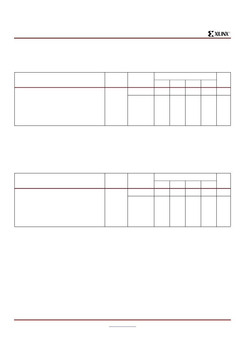
Virtex-E Pin-to-Pin Output Parameter Guidelines
All devices are 100% functionally tested. Listed below are representative values for typical pin locations and normal clock
loading. Values are expressed in nanoseconds unless otherwise noted.
Global Clock Input to Output Delay for LVTTL, 12 mA, Fast Slew Rate,
with
DLL
Global Clock Input to Output Delay for LVTTL, 12 mA, Fast Slew Rate,
without
DLL
Description
(1)
Symbol
Device
(3)
Speed Grade
(2)
Units
Min
-8
-7
-6
LVTTL Global Clock Input to Output Delay using
Output Flip-flop, 12 mA, Fast Slew Rate,
with
DLL.
For data
output
with different standards, adjust
the delays with the values shown in
‘‘IOB Output
Switching Characteristics Standard Adjustments’’
on page 8
.
T
ICKOFDLL
XCV405E
1.0
3.1
3.1
3.1
ns
XCV812E
1.0
3.1
3.1
3.1
ns
Notes:
1.
Listed above are representative values where one global clock input drives one vertical clock line in each accessible column, and
where all accessible IOB and CLB flip-flops are clocked by the global clock net.
Output timing is measured at 50% V
CC
threshold with 35 pF external capacitive load. For other I/O standards and different loads, see
Table 2
and
Table 3
.
DLL output jitter is already included in the timing calculation.
2.
3.
Description
(1)
Symbol
Device
Speed Grade
(2)
Units
Min
-8
-7
-6
LVTTL Global Clock Input to Output Delay using
Output Flip-flop, 12 mA, Fast Slew Rate,
without
DLL.
For data
output
with different standards, adjust
the delays with the values shown in
‘‘IOB Output
Switching Characteristics Standard Adjustments’’
on page 8
.
T
ICKOF
XCV405E
1.6
4.5
4.7
4.9
ns
XCV812E
1.8
4.8
5.0
5.2
ns
Notes:
1.
Listed above are representative values where one global clock input drives one vertical clock line in each accessible column, and
where all accessible IOB and CLB flip-flops are clocked by the global clock net.
Output timing is measured at 50% V
CC
threshold with 35 pF external capacitive load. For other I/O standards and different loads, see
Table 2
and
Table 3
.
2.
相關PDF資料 |
PDF描述 |
|---|---|
| XCV812E-6FG556I | Virtex-E 1.8 V Extended Memory Field Programmable Gate Arrays |
| XCV812E-6FG560C | Virtex-E 1.8 V Extended Memory Field Programmable Gate Arrays |
| XCV812E-6FG560I | Virtex-E 1.8 V Extended Memory Field Programmable Gate Arrays |
| XCV812E-6FG676C | Virtex-E 1.8 V Extended Memory Field Programmable Gate Arrays |
| XCV812E-6FG676I | Virtex-E 1.8 V Extended Memory Field Programmable Gate Arrays |
相關代理商/技術參數(shù) |
參數(shù)描述 |
|---|---|
| XCV812E-6FG556I | 制造商:XILINX 制造商全稱:XILINX 功能描述:Virtex-E 1.8 V Extended Memory Field Programmable Gate Arrays |
| XCV812E-6FG560C | 制造商:XILINX 制造商全稱:XILINX 功能描述:Virtex-E 1.8 V Extended Memory Field Programmable Gate Arrays |
| XCV812E-6FG560I | 制造商:XILINX 制造商全稱:XILINX 功能描述:Virtex-E 1.8 V Extended Memory Field Programmable Gate Arrays |
| XCV812E-6FG676C | 制造商:XILINX 制造商全稱:XILINX 功能描述:Virtex-E 1.8 V Extended Memory Field Programmable Gate Arrays |
| XCV812E-6FG676I | 制造商:XILINX 制造商全稱:XILINX 功能描述:Virtex-E 1.8 V Extended Memory Field Programmable Gate Arrays |
發(fā)布緊急采購,3分鐘左右您將得到回復。