- 您現(xiàn)在的位置:買賣IC網(wǎng) > PDF目錄375014 > XCR5128-7PQ100C (XILINX INC) 128 Macrocell CPLD PDF資料下載
參數(shù)資料
| 型號: | XCR5128-7PQ100C |
| 廠商: | XILINX INC |
| 元件分類: | PLD |
| 英文描述: | 128 Macrocell CPLD |
| 中文描述: | EE PLD, 9.5 ns, PQFP100 |
| 封裝: | PLASTIC, QFP-100 |
| 文件頁數(shù): | 7/20頁 |
| 文件大小: | 131K |
| 代理商: | XCR5128-7PQ100C |
R
XCR5128: 128 Macrocell CPLD
7
www.xilinx.com
1-800-255-7778
DS041 (v1.4) January 19, 2001
This product has been discontinued. Please see
www.xilinx.com/partinfo/notify/pdn0007.htm
for details.
JTAG Testing Capability
JTAG is the commonly-used acronym for the Boundary
Scan Test (BST) feature defined for integrated circuits by
IEEE Standard 1149.1. This standard defines input/output
pins, logic control functions, and commands which facilitate
both board and device level testing without the use of spe-
cialized test equipment. BST provides the ability to test the
external connections of a device, test the internal logic of
the device, and capture data from the device during normal
operation. BST provides a number of benefits in each of the
following areas:
Testability
-
Allows testing of an unlimited number of
interconnects on the printed circuit board
-
Testability is designed in at the component level
-
Enables desired signal levels to be set at specific
pins (Preload)
-
Data from pin or core logic signals can be examined
during normal operation
Reliability
-
Eliminates physical contacts common to existing test
fixtures (e.g., "bed-of-nails")
-
Degradation of test equipment is no longer a
concern
-
Facilitates the handling of smaller, surface-mount
components
-
Allows for testing when components exist on both
sides of the printed circuit board
Cost
-
Reduces/eliminates the need for expensive test
equipment
Reduces test preparation time
Reduces spare board inventories
-
-
The Xilinx XCR5128's JTAG interface includes a TAP Port
and a TAP Controller, both of which are defined by the IEEE
1149.1 JTAG Specification. As implemented in the Xilinx
XCR5128, the TAP Port includes four of the five pins (refer
to
Table 2
) described in the JTAG specification: TCK, TMS,
TDI, and TDO. The fifth signal defined by the JTAG specifi-
cation is TRST* (Test Reset). TRST* is considered an
optional signal, since it is not actually required to perform
BST or ISP. The Xilinx XCR5128 saves an I/O pin for gen-
eral purpose use by not implementing the optional TRST*
signal in the JTAG interface. Instead, the Xilinx XCR5128
supports the test reset functionality through the use of its
power up reset circuit, which is included in all Xilinx CPLDs.
The pins associated with the power up reset circuit should
connect to an external pull-up resistor to keep the JTAG
signals from floating when they are not being used.
In the Xilinx XCR5128, the four mandatory JTAG pins each
require a unique, dedicated pin on the device. However, if
JTAG and ISP are not desired in the end-application, these
pins may instead be used as additional general I/O pins.
The decision as to whether these pins are used for
JTAG/ISP or as general I/O is made when the JEDEC file is
generated. If the use of JTAG/ISP is selected, the dedi-
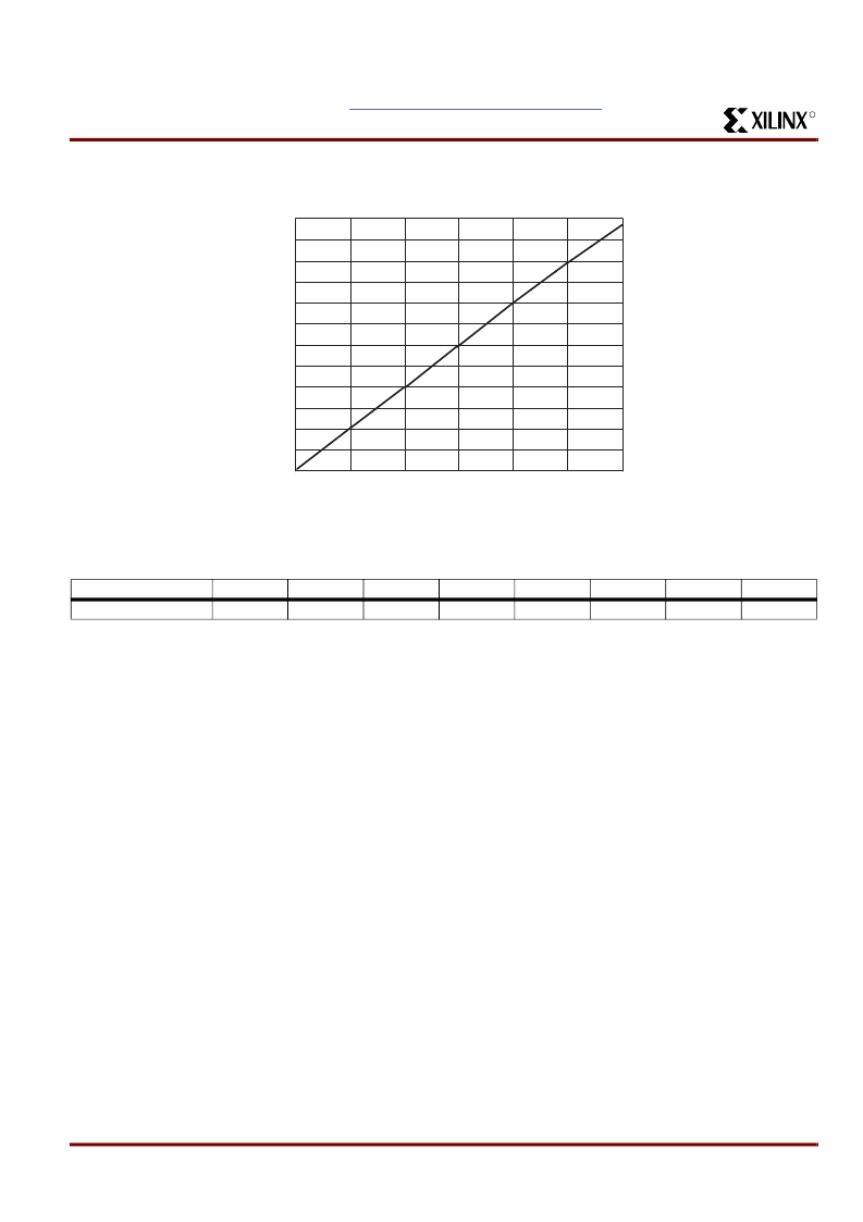
Table 1: I
CC
vs. Frequency
(V
CC
= 5V, 25
°
C)
Frequency (MHz)
Typical I
CC
(mA)
0
1
1
20
20
40
40
60
60
80
80
100
99
120
118
0.5
FREQUENCY (MHz)
SP00465
0
20
40
60
80
100
0
20
40
60
80
120
I
(mA)
100
120
Figure 5: I
CC
vs. Frequency at V
CC
= 5V, 25
°
C
相關(guān)PDF資料 |
PDF描述 |
|---|---|
| XCR5128-7PQ100I | 128 Macrocell CPLD |
| XCR5128-7PQ160C | 128 Macrocell CPLD |
| XCR5128-7PQ160I | 128 Macrocell CPLD |
| XCR5128-7TQ128C | 128 Macrocell CPLD |
| XCR5128-7TQ128I | 128 Macrocell CPLD |
相關(guān)代理商/技術(shù)參數(shù) |
參數(shù)描述 |
|---|---|
| XCR5128-7PQ100I | 制造商:XILINX 制造商全稱:XILINX 功能描述:128 Macrocell CPLD |
| XCR5128-7PQ160C | 制造商:XILINX 制造商全稱:XILINX 功能描述:128 Macrocell CPLD |
| XCR5128-7PQ160I | 制造商:XILINX 制造商全稱:XILINX 功能描述:128 Macrocell CPLD |
| XCR5128-7TQ128C | 制造商:XILINX 制造商全稱:XILINX 功能描述:128 Macrocell CPLD |
| XCR5128-7TQ128I | 制造商:XILINX 制造商全稱:XILINX 功能描述:128 Macrocell CPLD |
發(fā)布緊急采購,3分鐘左右您將得到回復(fù)。