- 您現(xiàn)在的位置:買賣IC網(wǎng) > PDF目錄375014 > XCR5128-15VQ100C (Xilinx, Inc.) 128 Macrocell CPLD PDF資料下載
參數(shù)資料
| 型號: | XCR5128-15VQ100C |
| 廠商: | Xilinx, Inc. |
| 英文描述: | 128 Macrocell CPLD |
| 中文描述: | 128個(gè)宏單元CPLD |
| 文件頁數(shù): | 11/20頁 |
| 文件大?。?/td> | 131K |
| 代理商: | XCR5128-15VQ100C |
R
XCR5128: 128 Macrocell CPLD
11
www.xilinx.com
1-800-255-7778
DS041 (v1.4) January 19, 2001
This product has been discontinued. Please see
www.xilinx.com/partinfo/notify/pdn0007.htm
for details.
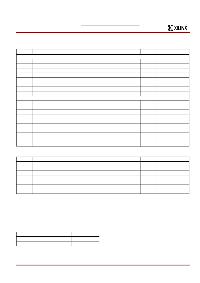
Programming Specifications
Absolute Maximum Ratings
1
Operating Range
Symbol
DC Parameters
V
CCP
I
CCP
V
IH
V
IL
V
SOL
V
SOH
TDO_I
OL
TDO_I
OH
AC Parameters
f
MAX
PWE
PWP
PWV
INIT
TMS_SU
TDI_SU
TMS_H
TDI_H
TDO_CO
Parameter
Min.
Max.
Unit
V
CC
supply program/verify
I
CC
limit program/verify
Input voltage (High)
Input voltage (Low)
Output voltage (Low)
Output voltage (High)
Output current (Low)
Output current (High)
4.5
5.5
200
V
mA
V
V
V
V
mA
mA
2.0
0.8
0.5
2.4
12
-12
CLK maximum frequency
Pulse width erase
Pulse width program
Pulse width verify
Initialization time
TMS setup time before TCK
↑
TDI setup time before TCK
↑
TMS hold time after TCK
↑
TDI hold time after TCK
↑
TDO valid after TCK
↓
10
100
10
10
100
10
10
20
20
MHz
ms
ms
μ
s
μ
s
ns
ns
ns
ns
ns
30
Symbol
V
CC
V
I
V
OUT
I
IN
I
OUT
T
J
T
str
Notes:
Parameter
Min.
-0.5
-1.2
-0.5
-30
-100
-40
-65
Max.
7.0
V
CC
+0.5
V
CC
+0.5
30
100
150
150
Unit
V
V
V
mA
mA
5
C
5
C
Supply voltage
2
Input voltage
Output voltage
Input current
Output current
Maximum junction temperature
Storage temperature
1. Stresses above those listed may cause malfunction or permanent damage to the device. This is a stress rating only.
Functional operation at these or any other condition above those indicated in the operational and programming specification
is not implied.
2. The chip supply voltage must rise monotonically.
Product Grade
Commercial
Industrial
Temperature
0 to +70
C
-40 to +85
°
C
Voltage
5.0V
+
5%
5.0V
+
10%
相關(guān)PDF資料 |
PDF描述 |
|---|---|
| XCR5128-15VQ100I | 128 Macrocell CPLD |
| XCR5128-7PC84C | 128 Macrocell CPLD |
| XCR5128-7PC84I | 128 Macrocell CPLD |
| XCR5128-7PQ100C | 128 Macrocell CPLD |
| XCR5128-7PQ100I | 128 Macrocell CPLD |
相關(guān)代理商/技術(shù)參數(shù) |
參數(shù)描述 |
|---|---|
| XCR5128-15VQ100I | 制造商:XILINX 制造商全稱:XILINX 功能描述:128 Macrocell CPLD |
| XCR5128-7PC84C | 制造商:XILINX 制造商全稱:XILINX 功能描述:128 Macrocell CPLD |
| XCR5128-7PC84I | 制造商:XILINX 制造商全稱:XILINX 功能描述:128 Macrocell CPLD |
| XCR5128-7PQ100C | 制造商:XILINX 制造商全稱:XILINX 功能描述:128 Macrocell CPLD |
| XCR5128-7PQ100I | 制造商:XILINX 制造商全稱:XILINX 功能描述:128 Macrocell CPLD |
發(fā)布緊急采購,3分鐘左右您將得到回復(fù)。