- 您現(xiàn)在的位置:買賣IC網(wǎng) > PDF目錄372881 > XCR3256XLSERIES 256 Macrocell CPLD PDF資料下載
參數(shù)資料
| 型號(hào): | XCR3256XLSERIES |
| 英文描述: | 256 Macrocell CPLD |
| 中文描述: | 256個(gè)宏單元CPLD |
| 文件頁數(shù): | 1/12頁 |
| 文件大?。?/td> | 113K |
| 代理商: | XCR3256XLSERIES |
DS013 (v1.9) January 8, 2002
Preliminary Product Specification
1-800-255-77781
2002 Xilinx, Inc. All rights reserved. All Xilinx trademarks, registered trademarks, patents, and disclaimers are as listed at
http://www.xilinx.com/legal.htm
.
All other trademarks and registered trademarks are the property of their respective owners. All specifications are subject to change without notice.
Features
Lowest power 256 macrocell CPLD
7.5 ns pin-to-pin logic delays
System frequencies up to 140 MHz
256 macrocells with 6,000 usable gates
Available in small footprint packages
-
144-pin TQFP (120 user I/O pins)
-
208-pin PQFP (164 user I/O)
-
256-ball FBGA (164 user I/O)
-
280-ball CS BGA (164 user I/O)
Optimized for 3.3V systems
-
Ultra low power operation
-
5V tolerant I/O pins with 3.3V core supply
-
Advanced 0.35 micron five layer metal EEPROM
process
-
Fast Zero Power (FZP) CMOS design
technology
Advanced system features
-
In-system programming
-
Input registers
-
Predictable timing model
-
Up to 23 clocks available per function block
-
Excellent pin retention during design changes
-
Full IEEE Standard 1149.1 boundary-scan (JTAG)
-
Four global clocks
-
Eight product term control terms per function block
Fast ISP programming times
Port Enable pin for additional I/O
2.7V to 3.6V supply voltage at industrial grade voltage
range
Programmable slew rate control per output
Security bit prevents unauthorized access
Refer to XPLA3 family data sheet (
DS012
) for
architecture description
Description
The XCR3256XL is a 3.3V, 256 macrocell CPLD targeted at
power sensitive designs that require leading edge program-
mable logic solutions. A total of 16 function blocks provide
6,000 usable gates. Pin-to-pin propagation delays are
7.5 ns with a maximum system frequency of 140 MHz.
TotalCMOS Design Technique for Fast
Zero Power
Xilinx offers a TotalCMOS CPLD, both in process technol-
ogy and design technique. Xilinx employs a cascade of
CMOS gates to implement its sum of products instead of
the traditional sense amp approach. This CMOS gate imple-
mentation allows Xilinx to offer CPLDs that are both high
performance and low power, breaking the paradigm that to
have low power, you must have low performance. Refer to
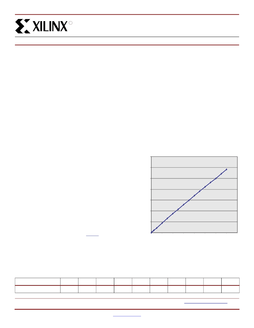
Figure 1
and
Table 1
showing the I
CC
vs. Frequency of our
XCR3256XL TotalCMOS CPLD (data taken with 16
resetable up/down, 16-bit counters at 3.3V, 25
°
C).
0
XCR3256XL 256 Macrocell CPLD
DS013 (v1.9) January 8, 2002
0
14
Preliminary Product Specification
R
Figure 1:
XCR3256XL Typical I
CC
vs. Frequency at
V
CC
= 3.3V, 25
°
C
0
20
40
60
80
100
120
140
0
DS013_01_102401
20
40
60
80
100
120
140 160
Frequency (MHz)
T
C
(
Table 1:
Typical I
CC
vs. Frequency at V
CC
= 3.3V, 25
°
C
Frequency (MHz)
0
1
10
20
40
60
80
100
120
140
Typical I
CC
(mA)
0.02
0.91
8.87
17.7
34.8
51.5
68
84.2
100.1
116.6
相關(guān)PDF資料 |
PDF描述 |
|---|---|
| XCR3320-10TQ144C | |
| XCR3320-7TQ144C | |
| XCR3320-8TQ144I | |
| XCR3384XLSERIES | 384 Macrocell CPLD |
| XCS05XL-4PC84C | Field Programmable Gate Array (FPGA) |
相關(guān)代理商/技術(shù)參數(shù) |
參數(shù)描述 |
|---|---|
| XCR3320-10TQ144C | 制造商:未知廠家 制造商全稱:未知廠家 功能描述: |
| XCR3320-7TQ144C | 制造商:未知廠家 制造商全稱:未知廠家 功能描述: |
| XCR3320-8TQ144I | 制造商:未知廠家 制造商全稱:未知廠家 功能描述: |
| XCR3384XL | 制造商:XILINX 制造商全稱:XILINX 功能描述:384 Macrocell CPLD |
| XCR3384XL_06 | 制造商:XILINX 制造商全稱:XILINX 功能描述:384 Macrocell CPLD |
發(fā)布緊急采購(gòu),3分鐘左右您將得到回復(fù)。