- 您現(xiàn)在的位置:買賣IC網(wǎng) > PDF目錄372876 > XC9511F1434 (TOREX SEMICONDUCTOR LTD.) Synchronous Step-Down DC/DC Converter with built-in LDO Regulator in parallel plus Voltage Detector PDF資料下載
參數(shù)資料
| 型號(hào): | XC9511F1434 |
| 廠商: | TOREX SEMICONDUCTOR LTD. |
| 英文描述: | Synchronous Step-Down DC/DC Converter with built-in LDO Regulator in parallel plus Voltage Detector |
| 中文描述: | 同步降壓型DC / DC轉(zhuǎn)換器內(nèi)置LDO的同時(shí)加電壓檢測(cè)器調(diào)節(jié)器 |
| 文件頁數(shù): | 5/35頁 |
| 文件大小: | 3471K |
| 代理商: | XC9511F1434 |
第1頁第2頁第3頁第4頁當(dāng)前第5頁第6頁第7頁第8頁第9頁第10頁第11頁第12頁第13頁第14頁第15頁第16頁第17頁第18頁第19頁第20頁第21頁第22頁第23頁第24頁第25頁第26頁第27頁第28頁第29頁第30頁第31頁第32頁第33頁第34頁第35頁
5/35
XC9511
Series
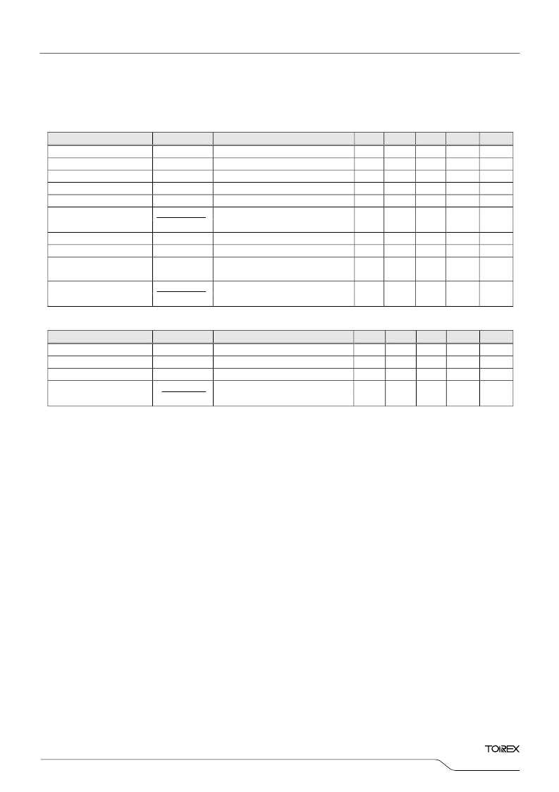
PARAMETER
SYMBOL
CONDITIONS
MIN.
TYP.
MAX.
UNITS
CIRCUIT
Output Voltage
Maximum Output Current
Load Regulation
VR
OUT
(E)
Imax2
U
VR
OUT
IR
OUT
=30mA
3.234
400
-
3.300
-
15
3.366
-
50
V
mA
mV
2
2
2
1mA
≦
IR
OUT
≦
100mA
IR
OUT
=100mA
Dropout Voltage 1 (*5)
Vdif 1
-
50
110
mV
2
Dropout Voltage 2
Vdif 2
U
VROUT
U
V
IN
VR
OUT
IR
OUT
=200mA
-
100
200
mV
2
IR
OUT
=30mA
Line Regulation
VR
OUT
(T)+1V
≦
V
IN
≦
6V
VR
OUT
=VR
OUT
(E) x 0.9
-
0.05
0.25
%/V
2
Current Limit
Ilim2
480
600
-
mA
7
Short-Circuit Current
Ishort
VR
OUT
=VSS
-
30
-
mA
7
Ripple Rejection Rate
PSRR
V
IN
={V
OUT
(T)+1.0} V
DC
+0.5Vp-pAC,
IR
OUT
=30mA, f=1kHz
IR
OUT
=30mA
-
60
-
dB
12
Output Voltage
Temperature Characteristics
U
VR
OUT
U
Topr
VR
OUT
-40
℃≦
Topr
≦
85
℃
-
±
100
-
ppm/
℃
2
PARAMETER
SYMBOL
CONDITIONS
MIN.
TYP.
MAX.
UNITS
CIRCUIT
Detect Voltage
Hysteresis Range
V
DF
(E)
V
HYS
CE=0V
V
HYS
=[V
DR
(E)
(*10)
- V
DF
(E)] / V
DF
(E) x 100
2.646
2
2.700
5
2.754
8
V
%
8
8
VD Output Current
IVD
U
V
DF
U
Topr
VDF
VDOUT=0.5V, CE=0V
1
-
-
mA
9
Output Voltage
Temperature Characteristics
-40
℃≦
Topr
≦
85
℃
-
±
100
-
ppm/
℃
8
■
ELECTRICAL CHARACTERISTICS (Continued)
●
Regulator (3.3V product)
Topr=25
℃
●
Detector (2.7V product)
Topr=25
℃
Test conditions: Unless otherwise stated:
DC/DC : VIN=3.6V [DC
OUT
:1.5V]
VR: V
IN
= 4.3V (V
IN
=VR
OUT
(T) + 1.0V)
VD: V
IN
=5.0V
Common conditions for all test items: CE=V
IN
, MODE=0V
* VR
OUT
(T) : Setting output voltage
NOTE:
*1: Including hysteresis operating voltage range.
*2: ON resistance (
Ω
)= 0.05 (V) / ILX (A).
*3: EFFI = { ( Output Voltage x Output Current ) / ( Input Voltage x Input Current) } x 100
*4: Time until it short-circuits DC
OUT
with GND through 1
Ω
of resistance from a state of operation and is set to DC
OUT
=0V from
current limit pulse generating.
*5: Vdif = (V
IN
1
(*6)
- VR
OUT
1
(*7)
)
*6: V
IN
1 = The input voltage when VROUT1 appears as input voltage is gradually decreased.
*7: VR
OUT
1 = A voltage equal to 98% of the output voltage whenever an amply stabilized I
OUT
{VR
OUT
(T) + 1.0V} is input.
*8: Current limit = When V
IN
is low, limit current may not be reached because of voltage falls caused by ON resistance or serial
resistance of coils.
*9: Integral latch circuit=latch time may become longer and latch operation may not work when V
IN
is 3.0V or more.
*10: V
DR(E)
= VD release voltage
*11: When temperature is high, a current of approximately 5.0
μ
A (maximum) may leak.
*12: When using the IC with a regulator output at almost no load, a capacitor should be placed as close as possible between
AVDD and AGND (C
IN
2), connected with low impedance. Please also see the recommended pattern layout on page 13
for your reference. Should it not be possible to place the input capacitor nearby, the regulated output level may increase
up to the V
DD
level while the load of the DC/DC converter increases and the regulator output is at almost no load.
XC9511xxxCSx (Continued)
相關(guān)PDF資料 |
PDF描述 |
|---|---|
| XC95144XLSERIES | High Performance CPLD |
| XC95288-10BG352C | Flash Complex PLD |
| XC95288-10HQ208C | Flash Complex PLD |
| XC95288-15BG352C | Flash Complex PLD |
| XC95288-15BG352I | Flash Complex PLD |
相關(guān)代理商/技術(shù)參數(shù) |
參數(shù)描述 |
|---|---|
| XC9511F143SRL | 制造商:TOREX 制造商全稱:Torex Semiconductor 功能描述:Synchronous Step-Down DC/DC Converter with built-in LDO Regulator in parallel plus Voltage Detector |
| XC9511F1463 | 制造商:TOREX 制造商全稱:Torex Semiconductor 功能描述:Synchronous Step-Down DC/DC Converter with built-in LDO Regulator in parallel plus Voltage Detector |
| XC9511F1464 | 制造商:TOREX 制造商全稱:Torex Semiconductor 功能描述:Synchronous Step-Down DC/DC Converter with built-in LDO Regulator in parallel plus Voltage Detector |
| XC9511F146SRL | 制造商:TOREX 制造商全稱:Torex Semiconductor 功能描述:Synchronous Step-Down DC/DC Converter with built-in LDO Regulator in parallel plus Voltage Detector |
| XC9511F14C3 | 制造商:TOREX 制造商全稱:Torex Semiconductor 功能描述:Synchronous Step-Down DC/DC Converter with built-in LDO Regulator in parallel plus Voltage Detector |
發(fā)布緊急采購,3分鐘左右您將得到回復(fù)。