- 您現(xiàn)在的位置:買賣IC網(wǎng) > PDF目錄372865 > XC9110A191MR (TOREX SEMICONDUCTOR LTD.) PFM Controlled Step-Up DC/DC Converter / Controller ICs PDF資料下載
參數(shù)資料
| 型號: | XC9110A191MR |
| 廠商: | TOREX SEMICONDUCTOR LTD. |
| 英文描述: | PFM Controlled Step-Up DC/DC Converter / Controller ICs |
| 中文描述: | 烤瓷控制升壓型DC / DC轉(zhuǎn)換器/控制器芯片 |
| 文件頁數(shù): | 6/35頁 |
| 文件大小: | 2432K |
| 代理商: | XC9110A191MR |
第1頁第2頁第3頁第4頁第5頁當(dāng)前第6頁第7頁第8頁第9頁第10頁第11頁第12頁第13頁第14頁第15頁第16頁第17頁第18頁第19頁第20頁第21頁第22頁第23頁第24頁第25頁第26頁第27頁第28頁第29頁第30頁第31頁第32頁第33頁第34頁第35頁
6/35
XC9110/XC9111
Series
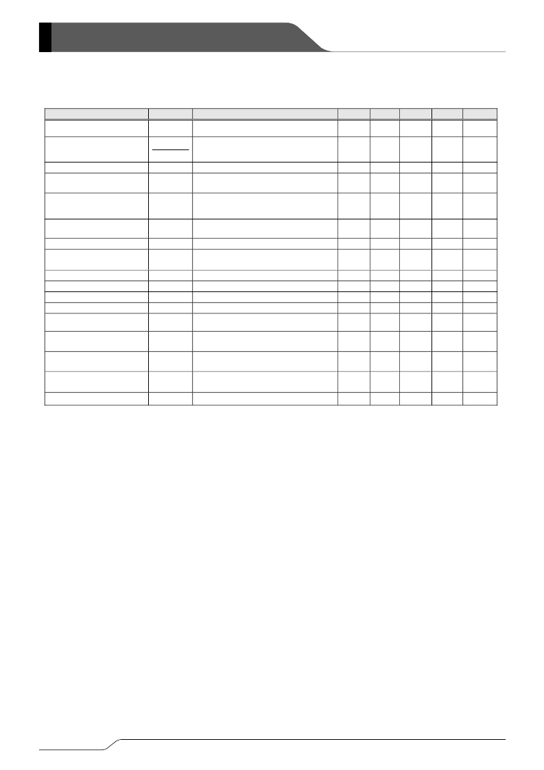
PARAMETER
SYMBOL
CONDITIONS
MIN.
TYP.
MAX.
UNIT
CIRCUIT
Output Voltage
V
OUT
Connected to external components
×
0.975
V
OUT
×
1.025
V
①
Output Voltage Temperature
Characteristics
△
V
OUT
△
V
OUT
△
topr
Connected to external components
- 40
℃≦
Topr
≦
85
℃
-
±
100
-
ppm/
℃
①
Maximum Input Voltage
V
IN
10
-
-
V
①
Operating Start Voltage
V
ST1
I
OUT
=1mA,
Connected to external components
-
0.8
0.9
V
①
Oscillation Start Voltage
V
ST2
Applied 0.8V to V
OUT
, Vpull=1.0V
-
-
0.8
V
②
Operating Hold Voltage
V
HLD
I
OUT
=1mA,
Connected to external components
I
OUT
=0mA (*1)
0.7
-
-
V
①
Input Current at No Load
I
IN
-
E1-1(*) E1-2(*)
μ
A
①
Supply Current 1 (*2)
I
DD1
Applied (output voltage
×
0.95) to V
OUT
-
E2-1(*) E2-2(*)
μ
A
②
Supply Current 2
Lx Switch ON Resistance
Lx Leak Current
Duty Ratio
I
DD2
RSWON
I
LxL
DTY
Applied (output voltage+0.5) to V
OUT
Same as I
DD1
, VLx=0.4V (*3)
Same as I
DD2
, VLx
=
7V
Same as I
DD1
, measure Lx waveform
I
OUT
=1mA, measure Lx ON time.
Connect to external components
-
-
-
E3-1(*) E3-2(*)
E4-1(*) E4-2(*)
-
E7-2(*) E7-3(*)
μ
A
Ω
μ
A
%
②
②
③
②
1
E7-1(*)
Duty Ratio 2
DTY2
48
56
64
%
①
Maximum Oscillation
Frequency
Maximum Oscillation
Frequency 2
MAXFOSC
Same as I
DD1
85
100
115
kHz
②
MAXFOSC2
Same as I
DD1
153
180
207
kHz
②
Lx Limit Voltage (*4)
V
LxLMT
Same as I
DD1
, VLx when max. oscillation
frequency is more than double
0.7
-
1.1
V
②
Efficiency (*5)
EFFI
Connect to external components
-
E8(*)
-
%
①
■
ELECTRICAL CHARACTERISTICS
XC9111Axx1MR
Test condition : Unless otherwise specified, V
IN
=V
OUT
×
0.6, I
OUT
=<C1(*)>, Vpull=5.0V
NOTE:
*1: TOREX SBD, XB01SB04A2BR is used, reverse current IR < 1
μ
A (when reverse voltage V
R
= 10V is applied), in case of using selected
parts.
*2: Supply Current 1 is the value when the IC is constantly switching. In actual operation, the oscillator periodically switches, resulting in
lower power consumption. Please refer to Input Current (I
IN
) under no load condition for the actual current, which is supplied from the
input power supply (V
IN
).
*3: Lx switch ON resistance can be calculated by (V
Lx
x Rp)
/
(Vpull - V
Lx
). * Change Vpull so that V
Lx
will become 0.4V.
*4: The Lx limit voltage function becomes stable when V
OUT
is over 2.0V.
*5: EFFI={[output voltage]
×
(output current)}
/
[(input voltage)
×
(input current)]
×
100
*6: Please be aware of the absolute maximum ratings of the external components.
(*): Please refer to the charts.
Ta = 25
℃
相關(guān)PDF資料 |
PDF描述 |
|---|---|
| XC9110A191PL | PFM Controlled Step-Up DC/DC Converter / Controller ICs |
| XC9110 | PFM Controlled Step-Up DC/DC Converter / Controller ICs |
| XC9110A151EL | PFM Controlled Step-Up DC/DC Converter / Controller ICs |
| XC9110A151ER | PFM Controlled Step-Up DC/DC Converter / Controller ICs |
| XC9110A151ML | PFM Controlled Step-Up DC/DC Converter / Controller ICs |
相關(guān)代理商/技術(shù)參數(shù) |
參數(shù)描述 |
|---|---|
| XC9110A191PL | 制造商:TOREX 制造商全稱:Torex Semiconductor 功能描述:PFM Controlled Step-Up DC/DC Converter / Controller ICs |
| XC9110A191PR | 制造商:TOREX 制造商全稱:Torex Semiconductor 功能描述:PFM Controlled Step-Up DC/DC Converter / Controller ICs |
| XC9110A301MR | 制造商:Torex Semiconductor LTD 功能描述: |
| XC9110A701EL | 制造商:TOREX 制造商全稱:Torex Semiconductor 功能描述:PFM Controlled Step-Up DC/DC Converter / Controller ICs |
| XC9110A701ER | 制造商:TOREX 制造商全稱:Torex Semiconductor 功能描述:PFM Controlled Step-Up DC/DC Converter / Controller ICs |
發(fā)布緊急采購,3分鐘左右您將得到回復(fù)。