- 您現(xiàn)在的位置:買賣IC網(wǎng) > PDF目錄4273 > XC3S1200E-5FTG256C (Xilinx Inc)IC FPGA SPARTAN3E 1200K 256FTBGA PDF資料下載
參數(shù)資料
| 型號(hào): | XC3S1200E-5FTG256C |
| 廠商: | Xilinx Inc |
| 文件頁數(shù): | 186/227頁 |
| 文件大?。?/td> | 0K |
| 描述: | IC FPGA SPARTAN3E 1200K 256FTBGA |
| 標(biāo)準(zhǔn)包裝: | 90 |
| 系列: | Spartan®-3E |
| LAB/CLB數(shù): | 2168 |
| 邏輯元件/單元數(shù): | 19512 |
| RAM 位總計(jì): | 516096 |
| 輸入/輸出數(shù): | 190 |
| 門數(shù): | 1200000 |
| 電源電壓: | 1.14 V ~ 1.26 V |
| 安裝類型: | 表面貼裝 |
| 工作溫度: | 0°C ~ 85°C |
| 封裝/外殼: | 256-LBGA |
| 供應(yīng)商設(shè)備封裝: | 256-FTBGA |
第1頁第2頁第3頁第4頁第5頁第6頁第7頁第8頁第9頁第10頁第11頁第12頁第13頁第14頁第15頁第16頁第17頁第18頁第19頁第20頁第21頁第22頁第23頁第24頁第25頁第26頁第27頁第28頁第29頁第30頁第31頁第32頁第33頁第34頁第35頁第36頁第37頁第38頁第39頁第40頁第41頁第42頁第43頁第44頁第45頁第46頁第47頁第48頁第49頁第50頁第51頁第52頁第53頁第54頁第55頁第56頁第57頁第58頁第59頁第60頁第61頁第62頁第63頁第64頁第65頁第66頁第67頁第68頁第69頁第70頁第71頁第72頁第73頁第74頁第75頁第76頁第77頁第78頁第79頁第80頁第81頁第82頁第83頁第84頁第85頁第86頁第87頁第88頁第89頁第90頁第91頁第92頁第93頁第94頁第95頁第96頁第97頁第98頁第99頁第100頁第101頁第102頁第103頁第104頁第105頁第106頁第107頁第108頁第109頁第110頁第111頁第112頁第113頁第114頁第115頁第116頁第117頁第118頁第119頁第120頁第121頁第122頁第123頁第124頁第125頁第126頁第127頁第128頁第129頁第130頁第131頁第132頁第133頁第134頁第135頁第136頁第137頁第138頁第139頁第140頁第141頁第142頁第143頁第144頁第145頁第146頁第147頁第148頁第149頁第150頁第151頁第152頁第153頁第154頁第155頁第156頁第157頁第158頁第159頁第160頁第161頁第162頁第163頁第164頁第165頁第166頁第167頁第168頁第169頁第170頁第171頁第172頁第173頁第174頁第175頁第176頁第177頁第178頁第179頁第180頁第181頁第182頁第183頁第184頁第185頁當(dāng)前第186頁第187頁第188頁第189頁第190頁第191頁第192頁第193頁第194頁第195頁第196頁第197頁第198頁第199頁第200頁第201頁第202頁第203頁第204頁第205頁第206頁第207頁第208頁第209頁第210頁第211頁第212頁第213頁第214頁第215頁第216頁第217頁第218頁第219頁第220頁第221頁第222頁第223頁第224頁第225頁第226頁第227頁
Spartan-3E FPGA Family: Functional Description
DS312 (v4.1) July 19, 2013
Product Specification
61
The connections for the bottom-edge BUFGMUX elements
are similar to the top-edge connections (see Figure 46).
On the left and right edges, only two clock inputs feed each
pair of BUFGMUX elements.
Quadrant Clock Routing
The clock routing within the FPGA is quadrant-based, as
shown in Figure 45. Each clock quadrant supports eight
total clock signals, labeled ‘A’ through ‘H’ in Table 41 and
Figure 47. The clock source for an individual clock line
originates either from a global BUFGMUX element along
the top and bottom edges or from a BUFGMUX element
along the associated edge, as shown in Figure 47. The
clock lines feed the synchronous resource elements (CLBs,
IOBs, block RAM, multipliers, and DCMs) within the
quadrant.
The four quadrants of the device are:
Top Right (TR)
Bottom Right (BR)
Bottom Left (BL)
Top Left (TL)
Note that the quadrant clock notation (TR, BR, BL, TL) is
separate from that used for similar IOB placement
constraints.
To estimate the quadrant location for a particular I/O, see
the footprint diagrams in Module 4, Pinout Descriptions. For
exact quadrant locations, use the floorplanning tool. In the
QFP packages (VQ100, TQ144 and PQ208) the quadrant
borders fall in the middle of each side of the package, at a
GND pin. The clock inputs fall on the quadrant boundaries,
as indicated in Table 42.
In a few cases, a dedicated input is physically in one
quadrant of the device but connects to a different clock
quadrant:
FT256, H16 is in clock quadrant BR
FG320, K2 is in clock quadrant BL
FG400, L8 is in clock quadrant TL and the I/O at N11 is
in clock quadrant BL
FG484, M2 is in clock quadrant TL and L15 is in clock
quadrant BR
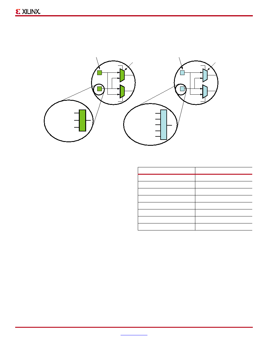
X-Ref Target - Figure 46
Figure 46: Clock Switch Matrix to BUFGMUX Pair Connectivity
BUFGMUX
LHCLK or
RHCLK input
Double Line
DCM output*
Left-/Right-Half BUFGMUX
CLK Switch
Matrix
S
O
S
I1
I0
I1
I0
BUFGMUX
Top/Bottom (Global) BUFGMUX
CLK Switch
Matrix
S
O
S
I1
I0
I1
I0
1st GCLK pin
2nd GCLK pin
1st DCM output
2nd DCM output
Double Line
DS312-2_16_110706
0
1
0
1
0
1
0
1
*(XC3S1200E and
XC3S1600E only)
Table 42: QFP Package Clock Quadrant Locations
Clock Pins
Quadrant
GCLK[3:0]
BR
GCLK[7:4]
TR
GCLK[11:8]
TL
GCLK[15:12]
BL
RHCLK[3:0]
BR
RHCLK[7:4]
TR
LHCLK[3:0]
TL
LHCLK[7:4]
BL
相關(guān)PDF資料 |
PDF描述 |
|---|---|
| ACC60DRXH | CONN EDGECARD 120PS .100 DIP SLD |
| GCB100DHAR | CONN EDGECARD 200PS R/A .050 SLD |
| 3341-25 | CONN JACKSOCKET M2.5/M2 0.41" |
| XC3S1200E-4FTG256I | IC FPGA SPARTAN3E 1200K 256FTBGA |
| XC6SLX25T-N3CSG324C | IC FPGA SPARTAN-6 324CSBGA |
相關(guān)代理商/技術(shù)參數(shù) |
參數(shù)描述 |
|---|---|
| XC3S1200E-5FTG256I | 制造商:XILINX 制造商全稱:XILINX 功能描述:Spartan-3E FPGA Family |
| XC3S1200E-5PQ208C | 制造商:XILINX 制造商全稱:XILINX 功能描述:Spartan-3E FPGA Family |
| XC3S1200E-5PQ208I | 制造商:XILINX 制造商全稱:XILINX 功能描述:Spartan-3E FPGA Family |
| XC3S1200E-5PQG208C | 制造商:XILINX 制造商全稱:XILINX 功能描述:Spartan-3E FPGA Family |
| XC3S1200E-5PQG208I | 制造商:XILINX 制造商全稱:XILINX 功能描述:Spartan-3E FPGA Family |
發(fā)布緊急采購,3分鐘左右您將得到回復(fù)。