- 您現(xiàn)在的位置:買賣IC網(wǎng) > PDF目錄374980 > XC3142L-3PC84C (XILINX INC) Field Programmable Gate Arrays (XC3000A/L, XC3100A/L) PDF資料下載
參數(shù)資料
| 型號: | XC3142L-3PC84C |
| 廠商: | XILINX INC |
| 元件分類: | FPGA |
| 英文描述: | Field Programmable Gate Arrays (XC3000A/L, XC3100A/L) |
| 中文描述: | FPGA, 144 CLBS, 2000 GATES, 270 MHz, PQCC84 |
| 封裝: | PLASTIC, LCC-84 |
| 文件頁數(shù): | 45/76頁 |
| 文件大小: | 731K |
| 代理商: | XC3142L-3PC84C |
第1頁第2頁第3頁第4頁第5頁第6頁第7頁第8頁第9頁第10頁第11頁第12頁第13頁第14頁第15頁第16頁第17頁第18頁第19頁第20頁第21頁第22頁第23頁第24頁第25頁第26頁第27頁第28頁第29頁第30頁第31頁第32頁第33頁第34頁第35頁第36頁第37頁第38頁第39頁第40頁第41頁第42頁第43頁第44頁當前第45頁第46頁第47頁第48頁第49頁第50頁第51頁第52頁第53頁第54頁第55頁第56頁第57頁第58頁第59頁第60頁第61頁第62頁第63頁第64頁第65頁第66頁第67頁第68頁第69頁第70頁第71頁第72頁第73頁第74頁第75頁第76頁
R
November 9, 1998 (Version 3.1)
7-47
XC3000 Series Field Programmable Gate Arrays
7
XC3000L Switching Characteristics
Xilinx maintains test specifications for each product as controlled documents. To insure the use of the most recently released
device performance parameters, please request a copy of the current test-specification revision.
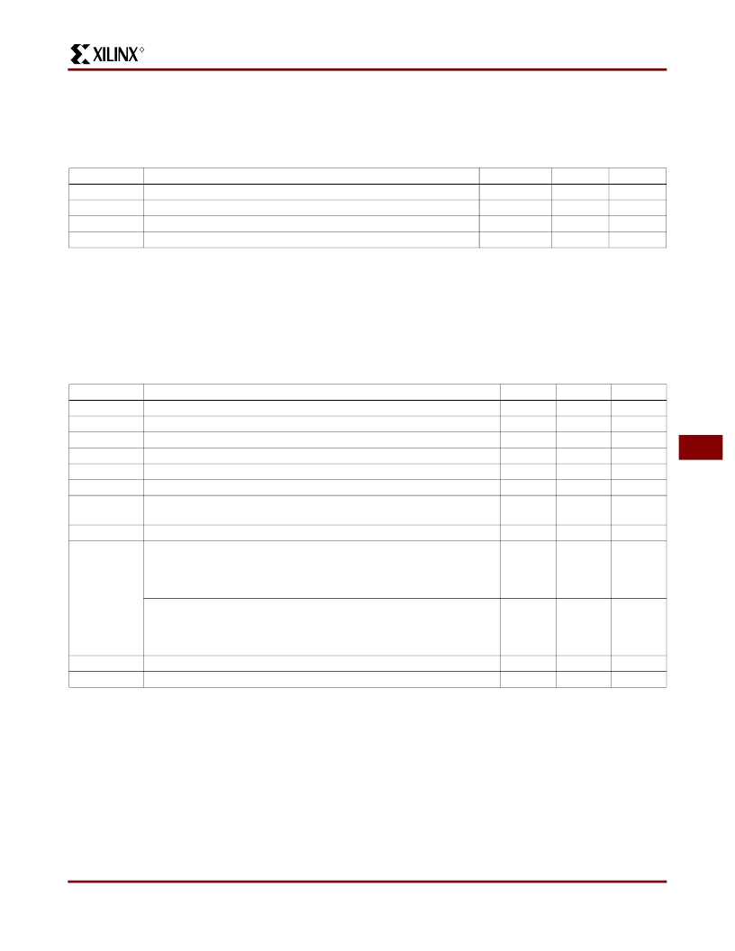
XC3000L Operating Conditions
Notes:
1. At junction temperatures above those listed as Operating Conditions, all delay parameters increase by 0.3% per
°
C.
2. Although the present (1996) devices operate over the full supply voltage range from 3.0 to 5.25 V, Xilinx reserves the right to
restrict operation to the 3.0 to 3.6 V range later, when smaller device geometries might preclude operation at 5V. Operating
conditions are guaranteed in the 3.0 – 3.6 V V
CC
range.
XC3000L DC Characteristics Over Operating Conditions
Notes:
1. With no output current loads, no active input or Longline pull-up resistors, all package pins at V
CC
or GND, and the FPGA
device configured with a tie option. I
is in addition to I
.
2. Total continuous output sink current may not exceed 100 mA per ground pin. Total continuous output source may not exceed
100 mA per V
pin. The number of ground pins varies from the XC3020L to the XC3090L.
3. Not tested. Allows an undriven pin to float High. For any other purpose, use an external pull-up.
Symbol
V
CC
V
IH
V
IL
T
IN
Description
Min
3.0
2.0
-0.3
Max
3.6
V
CC
+0.3
0.8
250
Units
V
V
V
ns
Supply voltage relative to GND Commercial 0
°
C to +85
°
C junction
High-level input voltage — TTL configuration
Low-level input voltage — TTL configuration
Input signal transition time
Symbol
V
OH
V
OL
V
OH
V
OL
V
CCPD
I
CCPD
Description
Min
2.40
Max
Units
V
V
V
V
V
μ
A
High-level output voltage (@ I
OH
= –4.0 mA, V
CC
min)
Low-level output voltage (@ I
OL
= 4.0 mA, V
CC
min)
High-level output voltage (@ I
OH
= –4.0 mA, V
CC
min)
Low-level output voltage (@ I
OL
= 4.0 mA, V
CC
min)
Power-down supply voltage (PWRDWN must be Low)
Power-down supply current (V
CC(MAX)
@ T
MAX
)
Quiescent FPGA supply current in addition to I
CCPD
Chip thresholds programmed as CMOS levels
Input Leakage Current
Input capacitance, all packages except PGA175
(sample tested)
All Pins except XTL1 and XTL2
XTL1 and XTL2
Input capacitance, PGA 175
(sample tested)
All Pins except XTL1 and XTL2
XTL1 and XTL2
Pad pull-up (when selected) @ V
IN
= 0 V
3
Horizontal Longline pull-up (when selected) @ logic Low
0.40
V
CC
-0.2
0.2
2.30
10
I
CCO
1
20
+10
μ
A
μ
A
I
IL
–10
C
IN
10
15
pF
pF
15
20
0.17
2.50
pF
pF
mA
mA
I
RIN
I
RLL
0.01
相關(guān)PDF資料 |
PDF描述 |
|---|---|
| XC3142L-3TQ144C | Field Programmable Gate Arrays (XC3000A/L, XC3100A/L) |
| XC3142L-3VQ160C | Field Programmable Gate Arrays (XC3000A/L, XC3100A/L) |
| XC3190L-2PC84C | Field Programmable Gate Arrays (XC3000A/L, XC3100A/L) |
| XC3190L-2TQ176C | Field Programmable Gate Arrays (XC3000A/L, XC3100A/L) |
| XC3190L-3PC84C | Field Programmable Gate Arrays (XC3000A/L, XC3100A/L) |
相關(guān)代理商/技術(shù)參數(shù) |
參數(shù)描述 |
|---|---|
| XC3142L-3TQ144C | 制造商:XILINX 制造商全稱:XILINX 功能描述:Field Programmable Gate Arrays (XC3000A/L, XC3100A/L) |
| XC3142L-3VQ160C | 制造商:XILINX 制造商全稱:XILINX 功能描述:Field Programmable Gate Arrays (XC3000A/L, XC3100A/L) |
| XC3142-PG132CPH | 制造商:Xilinx 功能描述: |
| XC3142-PG841PH | 制造商:Xilinx 功能描述: |
| XC3142-PG84CPH | 制造商:Xilinx 功能描述: |
發(fā)布緊急采購,3分鐘左右您將得到回復(fù)。