- 您現(xiàn)在的位置:買賣IC網(wǎng) > PDF目錄374980 > XC3064L-8PC84I (XILINX INC) Field Programmable Gate Arrays (XC3000A/L, XC3100A/L) PDF資料下載
參數(shù)資料
| 型號: | XC3064L-8PC84I |
| 廠商: | XILINX INC |
| 元件分類: | FPGA |
| 英文描述: | Field Programmable Gate Arrays (XC3000A/L, XC3100A/L) |
| 中文描述: | FPGA, 224 CLBS, 3500 GATES, 80 MHz, PQCC84 |
| 封裝: | PLASTIC, LCC-84 |
| 文件頁數(shù): | 28/76頁 |
| 文件大小: | 731K |
| 代理商: | XC3064L-8PC84I |
第1頁第2頁第3頁第4頁第5頁第6頁第7頁第8頁第9頁第10頁第11頁第12頁第13頁第14頁第15頁第16頁第17頁第18頁第19頁第20頁第21頁第22頁第23頁第24頁第25頁第26頁第27頁當(dāng)前第28頁第29頁第30頁第31頁第32頁第33頁第34頁第35頁第36頁第37頁第38頁第39頁第40頁第41頁第42頁第43頁第44頁第45頁第46頁第47頁第48頁第49頁第50頁第51頁第52頁第53頁第54頁第55頁第56頁第57頁第58頁第59頁第60頁第61頁第62頁第63頁第64頁第65頁第66頁第67頁第68頁第69頁第70頁第71頁第72頁第73頁第74頁第75頁第76頁
R
XC3000 Series Field Programmable Gate Arrays
7-30
November 9, 1998 (Version 3.1)
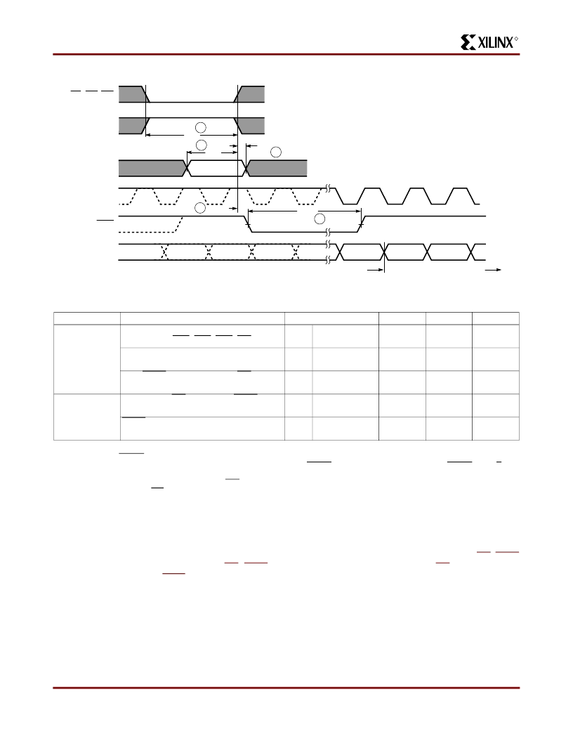
Notes:
1. At power-up, V
must rise from 2.0 V to V
min in less than 25 ms. If this is not possible, configuration can be delayed by
holding RESET Low until V
CC
has reached 4.0 V (2.5 V for the XC3000L). A very long V
rise time of >100 ms, or a
non-monotonically rising V
may require a >6-
μ
s High level on RESET, followed by a >6-
μ
s Low level on RESET and D/P
after V
has reached 4.0 V (2.5 V for the XC3000L).
2. Configuration must be delayed until the INIT of all FPGAs is High.
3. Time from end of WS to CCLK cycle for the new byte of data depends on completion of previous byte processing and the
phase of the internal timing generator for CCLK.
4. CCLK and DOUT timing is tested in slave mode.
5. T
indicates that the double-buffered parallel-to-serial converter is not yet ready to receive new data. The shortest T
BUSY
occurs when a byte is loaded into an empty parallel-to-serial converter. The longest TBUSY occurs when a new word is
loaded into the input register before the second-level buffer has started shifting out data.
Note:
This timing diagram shows very relaxed requirements: Data need not be held beyond the rising edge of WS. BUSY
will go active within 60 ns after the end of WS. BUSY will stay active for several microseconds. WS may be asserted
immediately after the end of BUSY.
Figure 28: Peripheral Mode Programming Switching Characteristics
6
BUSY
T
D6
DOUT
RDY/BUSY
D7
D0
D1
D2
4
WTRB
T
Valid
2
DC
T
1
CA
T
CCLK
D0-D7
CS2
WS, CS0, CS1
3
CD
T
WRITE TO FPGA
X5992
Previous Byte
New Byte
Description
Symbol
Min
100
Max
Units
ns
WRITE
Effective Write time required
(Assertion of CS0, CS1, CS2, WS)
DIN Setup time required
DIN Hold time required
RDY/BUSY delay after end of WS
1
T
CA
2
3
4
T
DC
T
CD
T
WTRB
60
0
ns
ns
ns
60
RDY
Earliest next WS after end of BUSY
5
T
RBWT
0
ns
BUSY Low time generated
6
T
BUSY
2.5
9
CCLK
periods
相關(guān)PDF資料 |
PDF描述 |
|---|---|
| XC3064L-8TQ144C | Field Programmable Gate Arrays (XC3000A/L, XC3100A/L) |
| XC3064L-8TQ144I | Field Programmable Gate Arrays (XC3000A/L, XC3100A/L) |
| XC3030A-6PC44C | Field Programmable Gate Arrays (XC3000A/L, XC3100A/L) |
| XC3030A-6PC68C | Field Programmable Gate Arrays (XC3000A/L, XC3100A/L) |
| XC3030A-6PC84C | Field Programmable Gate Arrays (XC3000A/L, XC3100A/L) |
相關(guān)代理商/技術(shù)參數(shù) |
參數(shù)描述 |
|---|---|
| XC3064L-8TQ144C | 功能描述:IC FPGA 3.3V C-TEMP 144-TQFP RoHS:否 類別:集成電路 (IC) >> 嵌入式 - FPGA(現(xiàn)場可編程門陣列) 系列:XC3000A/L 產(chǎn)品變化通告:XC4000(E,L) Discontinuation 01/April/2002 標(biāo)準(zhǔn)包裝:24 系列:XC4000E/X LAB/CLB數(shù):100 邏輯元件/單元數(shù):238 RAM 位總計:3200 輸入/輸出數(shù):80 門數(shù):3000 電源電壓:4.5 V ~ 5.5 V 安裝類型:表面貼裝 工作溫度:-40°C ~ 100°C 封裝/外殼:120-BCBGA 供應(yīng)商設(shè)備封裝:120-CPGA(34.55x34.55) |
| XC3064L-8TQ144I | 功能描述:IC FPGA 3.3V I-TEMP 144-TQFP RoHS:否 類別:集成電路 (IC) >> 嵌入式 - FPGA(現(xiàn)場可編程門陣列) 系列:XC3000A/L 產(chǎn)品變化通告:XC4000(E,L) Discontinuation 01/April/2002 標(biāo)準(zhǔn)包裝:24 系列:XC4000E/X LAB/CLB數(shù):100 邏輯元件/單元數(shù):238 RAM 位總計:3200 輸入/輸出數(shù):80 門數(shù):3000 電源電壓:4.5 V ~ 5.5 V 安裝類型:表面貼裝 工作溫度:-40°C ~ 100°C 封裝/外殼:120-BCBGA 供應(yīng)商設(shè)備封裝:120-CPGA(34.55x34.55) |
| XC3090 | 制造商:XILINX 制造商全稱:XILINX 功能描述:Logic Cell Array Families |
| XC3090-100CB164B | 制造商:Xilinx 功能描述: |
| XC3090-100CB164C | 制造商:未知廠家 制造商全稱:未知廠家 功能描述:Field Programmable Gate Array (FPGA) |
發(fā)布緊急采購,3分鐘左右您將得到回復(fù)。