- 您現(xiàn)在的位置:買賣IC網(wǎng) > PDF目錄374980 > XC3030L-8PC84I (XILINX INC) Field Programmable Gate Arrays (XC3000A/L, XC3100A/L) PDF資料下載
參數(shù)資料
| 型號(hào): | XC3030L-8PC84I |
| 廠商: | XILINX INC |
| 元件分類: | FPGA |
| 英文描述: | Field Programmable Gate Arrays (XC3000A/L, XC3100A/L) |
| 中文描述: | FPGA, 100 CLBS, 1500 GATES, 80 MHz, PQCC84 |
| 封裝: | PLASTIC, LCC-84 |
| 文件頁(yè)數(shù): | 18/76頁(yè) |
| 文件大小: | 731K |
| 代理商: | XC3030L-8PC84I |
第1頁(yè)第2頁(yè)第3頁(yè)第4頁(yè)第5頁(yè)第6頁(yè)第7頁(yè)第8頁(yè)第9頁(yè)第10頁(yè)第11頁(yè)第12頁(yè)第13頁(yè)第14頁(yè)第15頁(yè)第16頁(yè)第17頁(yè)當(dāng)前第18頁(yè)第19頁(yè)第20頁(yè)第21頁(yè)第22頁(yè)第23頁(yè)第24頁(yè)第25頁(yè)第26頁(yè)第27頁(yè)第28頁(yè)第29頁(yè)第30頁(yè)第31頁(yè)第32頁(yè)第33頁(yè)第34頁(yè)第35頁(yè)第36頁(yè)第37頁(yè)第38頁(yè)第39頁(yè)第40頁(yè)第41頁(yè)第42頁(yè)第43頁(yè)第44頁(yè)第45頁(yè)第46頁(yè)第47頁(yè)第48頁(yè)第49頁(yè)第50頁(yè)第51頁(yè)第52頁(yè)第53頁(yè)第54頁(yè)第55頁(yè)第56頁(yè)第57頁(yè)第58頁(yè)第59頁(yè)第60頁(yè)第61頁(yè)第62頁(yè)第63頁(yè)第64頁(yè)第65頁(yè)第66頁(yè)第67頁(yè)第68頁(yè)第69頁(yè)第70頁(yè)第71頁(yè)第72頁(yè)第73頁(yè)第74頁(yè)第75頁(yè)第76頁(yè)
R
XC3000 Series Field Programmable Gate Arrays
7-20
November 9, 1998 (Version 3.1)
A re-program is initiated.when a configured XC3000 series
device senses a High-to-Low transition and subsequent >6
μ
s Low level on the DONE/PROG package pin, or, if this
pin is externally held permanently Low, a High-to-Low tran-
sition and subsequent >6
μ
s Low time on the RESET pack-
age pin.
The device returns to the Clear state where the configura-
tion memory is cleared and mode lines re-sampled, as for
an aborted configuration. The complete configuration pro-
gram is cleared and loaded during each configuration pro-
gram cycle.
Length count control allows a system of multiple Field Pro-
grammable Gate Arrays, of assorted sizes, to begin opera-
tion in a synchronized fashion. The configuration program
generated by the development system begins with a pre-
amble of 111111110010 followed by a 24-bit length count
representing the total number of configuration clocks
needed to complete loading of the configuration pro-
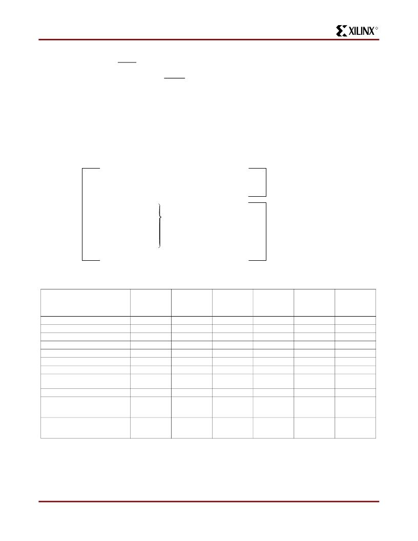
gram(s). The data framing is shown in
Figure 21
. All
FPGAs connected in series read and shift preamble and
length count in on positive and out on negative configura-
tion clock edges. A device which has received the pream-
ble and length count then presents a High Data Out until it
has intercepted the appropriate number of data frames.
When the configuration program memory of an FPGA is full
and the length count does not yet compare, the device
shifts any additional data through, as it did for preamble
and length count. When the FPGA configuration memory is
full and the length count compares, the device will execute
11111111
0010
< 24-Bit Length Count >
1111
0 <Data Frame # 001 > 111
0 <Data Frame # 002 > 111
0 <Data Frame # 003 > 111
. . .
. . .
. . .
0 <Data Frame # 196 > 111
0 <Data Frame # 197 > 111
1111
—Dummy Bits*
—Preamble Code
—Configuration Program Length
—Dummy Bits (4 Bits Minimum)
For XC3120
197 Configuration Data Frames
(Each Frame Consists of:
A Start Bit (0)
A 71-Bit Data Field
Three Stop Bits
Postamble Code (4 Bits Minimum)
Header
Program Data
Repeated for Each Logic
Cell Array in a Daisy Chain
*The LCA Device Require Four Dummy Bits Min; Software Generates Eight Dummy Bits
X5300_01
Figure 21: Internal Configuration Data Structure for an FPGA.
This shows the preamble, length count and data
frames generated by the Development System.
The Length Count produced by the program = [(40-bit preamble + sum of program data + 1 per daisy chain device)
rounded up to multiple of 8] – (2
≤
K
≤
4) where K is a function of DONE and RESET timing selected. An additional 8 is
added if roundup increment is less than K. K additional clocks are needed to complete start-up after length count is
reached.
Device
XC3020A
XC3020L
XC3120A
1,000 to 1,500
64
(8 x 8)
64
256
16
9
75
XC3030A
XC3030L
XC3130A
1,500 to 2,000
100
(10 x 10)
80
360
20
11
92
XC3042A
XC3042L
XC3142A
XC3142L
2,000 to 3,000
144
(12 x 12)
96
480
24
13
108
XC3064A
XC3064L
XC3164A
3,500 to 4,500
224
(16 x 14)
120
688
32
15
140
XC3090A
XC3090L
XC3190A
XC3190L
5,000 to 6,000
320
(20 x 16)
144
928
40
17
172
XC3195A
6,500 to 7,500
484
(22 x 22)
176
1,320
44
23
188
Gates
CLBs
Row x Col
IOBs
Flip-flops
Horizontal Longlines
TBUFs/Horizontal LL
Bits per Frame
(including1 start and 3 stop bits)
Frames
Program Data =
Bits x Frames + 4 bits
(excludes header)
PROM size (bits) =
Program Data
+ 40-bit Header
197
14,779
241
22,176
285
30,784
329
46,064
373
64,160
505
94,944
14,819
22,216
30,824
46,104
64,200
94,984
相關(guān)PDF資料 |
PDF描述 |
|---|---|
| XC3043L | Field Programmable Gate Arrays(現(xiàn)場(chǎng)可編程門陣列) |
| XC3030A-6PQ100C | Field Programmable Gate Arrays (XC3000A/L, XC3100A/L) |
| XC3142L-2PC84C | XTAL MTL T/H HC49/US |
| XC3142L-3PC84C | Field Programmable Gate Arrays (XC3000A/L, XC3100A/L) |
| XC3142L-3TQ144C | Field Programmable Gate Arrays (XC3000A/L, XC3100A/L) |
相關(guān)代理商/技術(shù)參數(shù) |
參數(shù)描述 |
|---|---|
| XC3030L-8VQ100C | 制造商:XILINX 制造商全稱:XILINX 功能描述:Field Programmable Gate Arrays (XC3000A/L, XC3100A/L) |
| XC3030L-8VQ100I | 制造商:XILINX 制造商全稱:XILINX 功能描述:Field Programmable Gate Arrays (XC3000A/L, XC3100A/L) |
| XC3030L-8VQ64C | 功能描述:IC FPGA C-TEMP 3.3V 64-VQFP RoHS:否 類別:集成電路 (IC) >> 嵌入式 - FPGA(現(xiàn)場(chǎng)可編程門陣列) 系列:XC3000A/L 產(chǎn)品變化通告:XC4000(E,L) Discontinuation 01/April/2002 標(biāo)準(zhǔn)包裝:24 系列:XC4000E/X LAB/CLB數(shù):100 邏輯元件/單元數(shù):238 RAM 位總計(jì):3200 輸入/輸出數(shù):80 門數(shù):3000 電源電壓:4.5 V ~ 5.5 V 安裝類型:表面貼裝 工作溫度:-40°C ~ 100°C 封裝/外殼:120-BCBGA 供應(yīng)商設(shè)備封裝:120-CPGA(34.55x34.55) |
| XC3030L-8VQ64I | 功能描述:IC FPGA I-TEMP 3.3V 64-VQFP RoHS:否 類別:集成電路 (IC) >> 嵌入式 - FPGA(現(xiàn)場(chǎng)可編程門陣列) 系列:XC3000A/L 產(chǎn)品變化通告:XC4000(E,L) Discontinuation 01/April/2002 標(biāo)準(zhǔn)包裝:24 系列:XC4000E/X LAB/CLB數(shù):100 邏輯元件/單元數(shù):238 RAM 位總計(jì):3200 輸入/輸出數(shù):80 門數(shù):3000 電源電壓:4.5 V ~ 5.5 V 安裝類型:表面貼裝 工作溫度:-40°C ~ 100°C 封裝/外殼:120-BCBGA 供應(yīng)商設(shè)備封裝:120-CPGA(34.55x34.55) |
| XC3042 | 制造商:Xilinx 功能描述: |
發(fā)布緊急采購(gòu),3分鐘左右您將得到回復(fù)。