- 您現(xiàn)在的位置:買賣IC網(wǎng) > PDF目錄4289 > XA3S250E-4VQG100Q (Xilinx Inc)IC FPGA SPARTAN-3E 250K 100-VQFP PDF資料下載
參數(shù)資料
| 型號: | XA3S250E-4VQG100Q |
| 廠商: | Xilinx Inc |
| 文件頁數(shù): | 6/37頁 |
| 文件大小: | 0K |
| 描述: | IC FPGA SPARTAN-3E 250K 100-VQFP |
| 標(biāo)準(zhǔn)包裝: | 90 |
| 系列: | Spartan®-3E XA |
| LAB/CLB數(shù): | 612 |
| 邏輯元件/單元數(shù): | 5508 |
| RAM 位總計: | 221184 |
| 輸入/輸出數(shù): | 66 |
| 門數(shù): | 250000 |
| 電源電壓: | 1.14 V ~ 1.26 V |
| 安裝類型: | 表面貼裝 |
| 工作溫度: | -40°C ~ 125°C |
| 封裝/外殼: | 100-TQFP |
| 供應(yīng)商設(shè)備封裝: | 100-VQFP(14x14) |
第1頁第2頁第3頁第4頁第5頁當(dāng)前第6頁第7頁第8頁第9頁第10頁第11頁第12頁第13頁第14頁第15頁第16頁第17頁第18頁第19頁第20頁第21頁第22頁第23頁第24頁第25頁第26頁第27頁第28頁第29頁第30頁第31頁第32頁第33頁第34頁第35頁第36頁第37頁
DS635 (v2.0) September 9, 2009
Product Specification
14
R
Switching Characteristics
I/O Timing
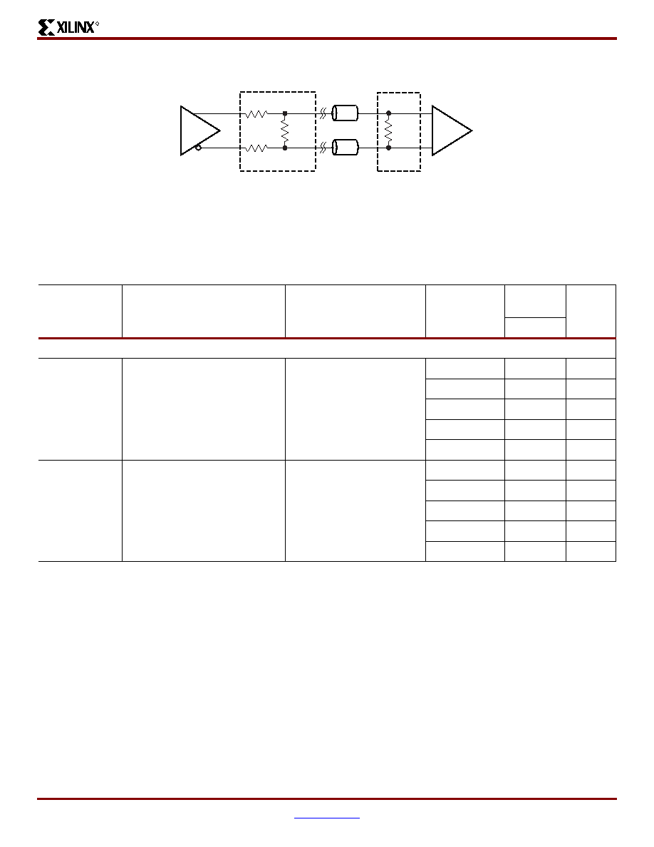
Figure 5: External Termination Resistors for BLVDS Transmitter and BLVDS Receiver
Z0 = 50
Ω
Z0 = 50
Ω
140
Ω
165
Ω
165
Ω
100
Ω
DS635_05_082807
VCCO = 2.5V
1/4th of Bourns
Part Number
CAT16-LV4F12
VCCO = 2.5V
1/4th of Bourns
Part Number
CAT16-PT4F4
Table 13: Pin-to-Pin Clock-to-Output Times for the IOB Output Path
Symbol
Description
Conditions
Device
-4 Speed
Grade
Units
Max
Clock-to-Output Times
TICKOFDCM
When reading from the Output
Flip-Flop (OFF), the time from
the active transition on the
Global Clock pin to data
appearing at the Output pin. The
DCM is used.
LVCMOS25(2), 12mA
output drive, Fast slew rate,
with DCM(3)
XA3S100E
2.79
ns
XA3S250E
3.45
ns
XA3S500E
3.46
ns
XA3S1200E
3.46
ns
XA3S1600E
3.45
ns
TICKOF
When reading from OFF, the
time from the active transition on
the Global Clock pin to data
appearing at the Output pin. The
DCM is not used.
LVCMOS25(2), 12mA
output drive, Fast slew rate,
without DCM
XA3S100E
5.92
ns
XA3S250E
5.43
ns
XA3S500E
5.51
ns
XA3S1200E
5.94
ns
XA3S1600E
6.05
ns
Notes:
1.
The numbers in this table are tested using the methodology presented in Table 19 and are based on the operating conditions set forth in
2.
This clock-to-output time requires adjustment whenever a signal standard other than LVCMOS25 is assigned to the Global Clock Input or a
standard other than LVCMOS25 with 12 mA drive and Fast slew rate is assigned to the data Output. If the former is true, add the appropriate
Input adjustment from Table 17. If the latter is true, add the appropriate Output adjustment from Table 18.
3.
DCM output jitter is included in all measurements.
4.
For minimums, use the values reported by the Xilinx timing analyzer.
相關(guān)PDF資料 |
PDF描述 |
|---|---|
| XC3S400A-5FTG256C | IC SPARTAN-3A FPGA 400K 256FTBGA |
| RBB120DHBN | CONN EDGECARD 240PS R/A .050 DIP |
| XC3S400A-5FT256C | IC SPARTAN-3A FPGA 400K 256FTBGA |
| EHHD15MF | CONN DSUB 15PIN MALE-FMALE |
| 93LC86CT-I/SN | IC EEPROM 16KBIT 3MHZ 8SOIC |
相關(guān)代理商/技術(shù)參數(shù) |
參數(shù)描述 |
|---|---|
| XA3S400-4FGG456I | 功能描述:IC FPGA SPARTAN-3 400K 456-FBGA RoHS:是 類別:集成電路 (IC) >> 嵌入式 - FPGA(現(xiàn)場可編程門陣列) 系列:Spartan®-3 XA 標(biāo)準(zhǔn)包裝:40 系列:Spartan® 6 LX LAB/CLB數(shù):3411 邏輯元件/單元數(shù):43661 RAM 位總計:2138112 輸入/輸出數(shù):358 門數(shù):- 電源電壓:1.14 V ~ 1.26 V 安裝類型:表面貼裝 工作溫度:-40°C ~ 100°C 封裝/外殼:676-BGA 供應(yīng)商設(shè)備封裝:676-FBGA(27x27) |
| XA3S400-4FGG456Q | 功能描述:IC FPGA SPARTAN-3 400K 456-FBGA RoHS:是 類別:集成電路 (IC) >> 嵌入式 - FPGA(現(xiàn)場可編程門陣列) 系列:Spartan®-3 XA 標(biāo)準(zhǔn)包裝:40 系列:Spartan® 6 LX LAB/CLB數(shù):3411 邏輯元件/單元數(shù):43661 RAM 位總計:2138112 輸入/輸出數(shù):358 門數(shù):- 電源電壓:1.14 V ~ 1.26 V 安裝類型:表面貼裝 工作溫度:-40°C ~ 100°C 封裝/外殼:676-BGA 供應(yīng)商設(shè)備封裝:676-FBGA(27x27) |
| XA3S400-4FTG256I | 功能描述:IC FPGA SPARTAN-3 400K 256-FTBGA RoHS:是 類別:集成電路 (IC) >> 嵌入式 - FPGA(現(xiàn)場可編程門陣列) 系列:Spartan®-3 XA 標(biāo)準(zhǔn)包裝:40 系列:Spartan® 6 LX LAB/CLB數(shù):3411 邏輯元件/單元數(shù):43661 RAM 位總計:2138112 輸入/輸出數(shù):358 門數(shù):- 電源電壓:1.14 V ~ 1.26 V 安裝類型:表面貼裝 工作溫度:-40°C ~ 100°C 封裝/外殼:676-BGA 供應(yīng)商設(shè)備封裝:676-FBGA(27x27) |
| XA3S400-4FTG256Q | 功能描述:IC FPGA SPARTAN-3 400K 256-FTBGA RoHS:是 類別:集成電路 (IC) >> 嵌入式 - FPGA(現(xiàn)場可編程門陣列) 系列:Spartan®-3 XA 標(biāo)準(zhǔn)包裝:40 系列:Spartan® 6 LX LAB/CLB數(shù):3411 邏輯元件/單元數(shù):43661 RAM 位總計:2138112 輸入/輸出數(shù):358 門數(shù):- 電源電壓:1.14 V ~ 1.26 V 安裝類型:表面貼裝 工作溫度:-40°C ~ 100°C 封裝/外殼:676-BGA 供應(yīng)商設(shè)備封裝:676-FBGA(27x27) |
| XA3S400-4PQG208I | 功能描述:IC FPGA SPARTAN-3 400K 208-PQFP RoHS:是 類別:集成電路 (IC) >> 嵌入式 - FPGA(現(xiàn)場可編程門陣列) 系列:Spartan®-3 XA 標(biāo)準(zhǔn)包裝:40 系列:Spartan® 6 LX LAB/CLB數(shù):3411 邏輯元件/單元數(shù):43661 RAM 位總計:2138112 輸入/輸出數(shù):358 門數(shù):- 電源電壓:1.14 V ~ 1.26 V 安裝類型:表面貼裝 工作溫度:-40°C ~ 100°C 封裝/外殼:676-BGA 供應(yīng)商設(shè)備封裝:676-FBGA(27x27) |
發(fā)布緊急采購,3分鐘左右您將得到回復(fù)。