- 您現(xiàn)在的位置:買賣IC網(wǎng) > PDF目錄371304 > X9530B15I Temperature Compensated Laser Diode Controller PDF資料下載
參數(shù)資料
| 型號: | X9530B15I |
| 英文描述: | Temperature Compensated Laser Diode Controller |
| 中文描述: | 溫度補償激光二極管控制器 |
| 文件頁數(shù): | 9/30頁 |
| 文件大小: | 479K |
| 代理商: | X9530B15I |
第1頁第2頁第3頁第4頁第5頁第6頁第7頁第8頁當(dāng)前第9頁第10頁第11頁第12頁第13頁第14頁第15頁第16頁第17頁第18頁第19頁第20頁第21頁第22頁第23頁第24頁第25頁第26頁第27頁第28頁第29頁第30頁
X9530
Characteristics subject to change without notice.
9 of 30
REV 3.7 8/26/04
www.xicor.com
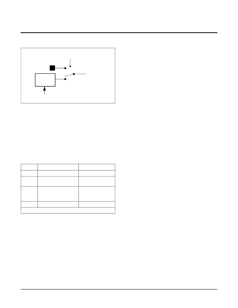
Figure 4. A/D Converter Input Select Structure
A/D Converter Range
From Figure 3 we can see that the operating range of
the A/D converter input depends on the voltage
reference. And from Figure 4 we see that the internal
temperature Sensor output also varies with the voltage
reference (VRef).
The table below summarizes the voltage range
restrictions on the VSense and VRef pins in different
configurations :
VSense and VRef ranges
LOOK-UP TABLES
The X9530 memory array contains two 64-byte look-up
tables. One is associated to pin I1’s output current
generator and the other to pin I2’s output current
generator, through their corresponding D/A converters.
The output of each look-up table is the byte contained
in the selected row. By default these bytes are the
inputs to the D/A converters driving pins I1 and I2.
The byte address of the selected row is obtained by
adding the look-up table base address (90h for LUT1,
and D0h for LUT2) and the appropriate row selection
bits. See Figure 6.
By default the look-up table selection bits are the 6-bit
output of the A/D converter. Alternatively, the A/D
converter can be bypassed and the six row selection
bits are the six LSBs of Control Registers 1 and 2, for
the LUT1 and LUT2 respectively. The selection
between these options is illustrated in Figure 7, and
described in “I2DS: Current Generator 2 Direction
Select Bit (Non-volatile)” on page 6, and “Control
Register 2” on page 6.
CURRENT GENERATOR BLOCK
The Current Generator pins I1 and I2 are outputs of
two independent current mode D/A converters.
D/A Converter Operation
The Block Diagram for each of the D/A converters is
shown in Figure 5.
The input byte of the D/A converter selects a voltage
on the non-inverting input of an operational amplifier.
The output of the amplifier drives the gate of a FET,
whose source is connected to ground via resistor R1.
This node is also fed back to the inverting input of the
amplifier. The drain of the FET is connected to the
output current pin (I1) via a “polarity select” circuit
block.
VRef
Internal
Internal
A/D Converter Input
Internal Temp. Sensor
VSense Pin
Ranges
Not Applicable
0
≤
V(VSense)
≤
V(VRef)
0
≤
V(VRef)
≤
1.3 V
0
≤
V(VSense)
≤
V(VRef)
Not a Valid Case
External
VSense Pin
External
All voltages referred to Vss.
Internal Temp. Sensor
VSense
Pin
On-chip
Temperature
Sensor
To A/D
Converter
Input
ADCIN: bit 3 in Control register 0.
VRef
相關(guān)PDF資料 |
PDF描述 |
|---|---|
| X9530B15I-T2 | Temperature Compensated Laser Diode Controller |
| X9530B15I-T1 | SINGLEMODE FIBER PATCH CABLE, PLENUM SC-LC 5M |
| X9530V14I | Temperature Compensated Laser Diode Controller |
| X9530-B15I | Temperature Compensated Laser Diode Controller |
| X9530B15I | Temperature Compensated Laser Diode Controller |
相關(guān)代理商/技術(shù)參數(shù) |
參數(shù)描述 |
|---|---|
| X9530-B15I | 制造商:INTERSIL 制造商全稱:Intersil Corporation 功能描述:Temperature Compensated Laser Diode Controller |
| X9530B15I-T1 | 制造商:INTERSIL 制造商全稱:Intersil Corporation 功能描述:Temperature Compensated Laser Diode Controller |
| X9530B15I-T2 | 制造商:INTERSIL 制造商全稱:Intersil Corporation 功能描述:Temperature Compensated Laser Diode Controller |
| X9530V14I | 功能描述:IC LASR CTRLR 1CHAN 5.5V 14TSSOP RoHS:否 類別:集成電路 (IC) >> PMIC - 激光驅(qū)動器 系列:- 產(chǎn)品培訓(xùn)模塊:Lead (SnPb) Finish for COTS Obsolescence Mitigation Program 標(biāo)準(zhǔn)包裝:60 系列:- 類型:激光二極管驅(qū)動器 數(shù)據(jù)速率:- 通道數(shù):4 電源電壓:3.3V 電流 - 電源:- 電流 - 調(diào)制:- 電流 - 偏置:- 工作溫度:0°C ~ 70°C 封裝/外殼:40-TQFN 裸露焊盤 供應(yīng)商設(shè)備封裝:40-TQFN EP 包裝:托盤 安裝類型:表面貼裝 |
| X9530-V14I | 制造商:INTERSIL 制造商全稱:Intersil Corporation 功能描述:Temperature Compensated Laser Diode Controller |
發(fā)布緊急采購,3分鐘左右您將得到回復(fù)。