- 您現(xiàn)在的位置:買賣IC網(wǎng) > PDF目錄371304 > X9530 Temperature Compensated Laser Diode Controller PDF資料下載
參數(shù)資料
| 型號: | X9530 |
| 英文描述: | Temperature Compensated Laser Diode Controller |
| 中文描述: | 溫度補(bǔ)償激光二極管控制器 |
| 文件頁數(shù): | 24/30頁 |
| 文件大小: | 479K |
| 代理商: | X9530 |
第1頁第2頁第3頁第4頁第5頁第6頁第7頁第8頁第9頁第10頁第11頁第12頁第13頁第14頁第15頁第16頁第17頁第18頁第19頁第20頁第21頁第22頁第23頁當(dāng)前第24頁第25頁第26頁第27頁第28頁第29頁第30頁
X9530
Characteristics subject to change without notice.
24 of 30
REV 3.7 8/26/04
www.xicor.com
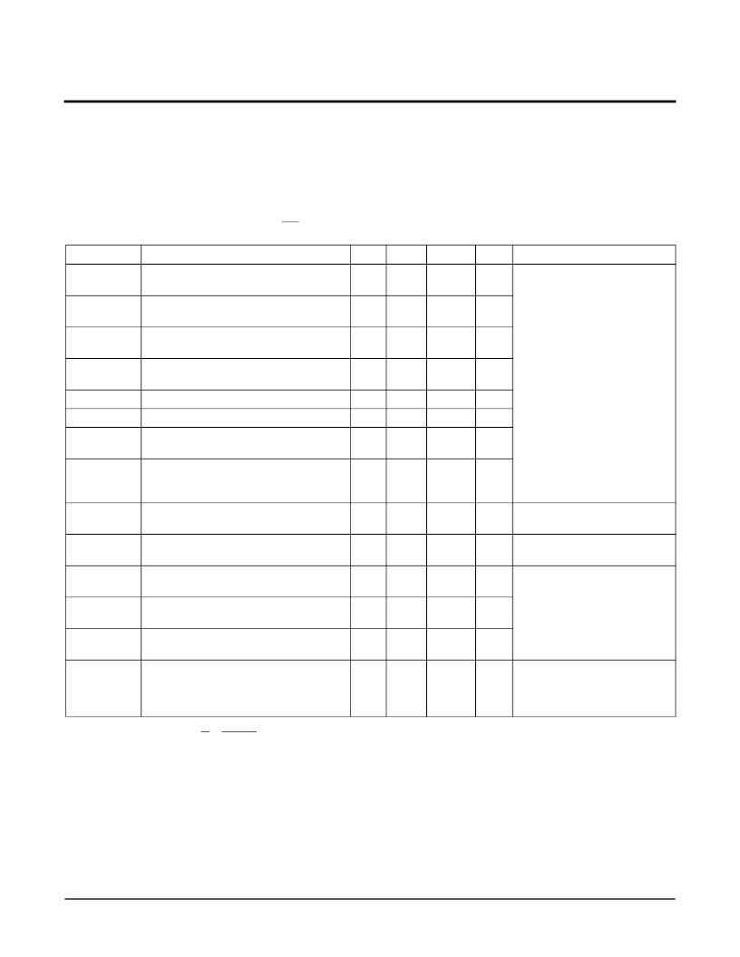
D/A CONVERTER CHARACTERISTICS
All typical values are for 25°C ambient temperature and 5 V at pin Vcc. Maximum and minimum specifications are over
the recommended operating conditions. All voltages are referred to the voltage at pin Vss unless otherwise specified. All
bits in control registers are “0” unless otherwise specified. 510, 0.1%, resistor connected between R1 and Vss, and
another between R2 and Vss unless otherwise specified. 400kHz TTL input at SCL unless otherwise specified. SDA
pulled to Vcc through an external 2K resistor unless otherwise specified. 2-wire interface in “standby” (see notes 1 and
2 on page 22), unless otherwise specified. WP A0, A1, and A2 floating unless otherwise specified.
Notes:
1. LSB is defined as
divided by the resistance between R1 or R2 to Vss.
2. Offset
DAC
: The Offset of a DAC is defined as the deviation between the measured and ideal output, when the DAC input is 01h. It is
expressed in LSB.
FSError
DAC
: The Full Scale Error of a DAC is defined as the deviation between the measured and ideal output, when the input is
FFh. It is expressed in LSB. The Offset
DAC
is subtracted from the measured value before calculating FSError
DAC
.
DNL
DAC
: The Differential Non-Linearity of a DAC is defined as the deviation between the measured and ideal incremental change in
the output of the DAC, when the input changes by one code step. It is expressed in LSB. The measured values are adjusted for Off-
set and Full Scale Error before calculating DNL
DAC
.
INL
DAC
: The Integral Non-Linearity of a DAC is defined as the deviation between the measured and ideal transfer curves, after
adjusting the measured transfer curve for Offset and Full Scale Error. It is expressed in LSB.
3.
These parameters are periodically sampled and not 100% tested.
Symbol
IFS
00
Parameter
Min
1.56
Typ
1.58
Max
1.6
Unit
mA
Test Conditions / Notes
DAC input Byte = FFh,
Source or sink mode, V(I1)
and V(I2) are Vcc–1.2V in
source mode and 1.2V in sink
mode.
See notes 1 and 2.
I1 or I2 full scale current, with external
resistor setting
I1 or I2 full scale current, with internal
low current setting option
I1 or I2 full scale current, with internal
middle current setting option
I1 or I2 full scale current, with internal
high current setting option
I1 or I2 D/A converter offset error
I1 or I2 D/A converter full scale error
I1 or I2 D/A converter
Differential Nonlinearity
I1 or I2 D/A converter Integral Nonlin-
earity with respect to a straight line
through 0 and the full scale value
I1 or I2 Sink Voltage Compliance
IFS
01
0.3
0.4
0.5
mA
IFS
10
0.64
0.85
1.06
mA
IFS
11
1
1.3
1.6
mA
Offset
DAC
FSError
DAC
DNL
DAC
1
-2
-0.5
1
2
LSB
LSB
LSB
0.5
INL
DAC
-1
1
LSB
VISink
1.2
Vcc
V
In this range the current at I1
or I2 vary < 1%
In this range the current at I1
or I2 vary < 1%
DAC input byte changing
from 00h to FFh and vice
versa, V(I1) and V(I2) are
Vcc–1.2V in source mode
and 1.2V in sink mode.
See note 3.
VISource
I1 or I2 Source Voltage Compliance
0
Vcc-1.2
V
I
OVER
I1 or I2 overshoot on D/A Converter
data byte transition
I1 or I2 undershoot on D/A Converter
data byte transition
I1 or I2 rise time on D/A Converter data
byte transition; 10% to 90%
Temperataure coefficient of output
current I1 or I2 when using internal
resistor setting
0
μ
A
I
UNDER
0
μ
A
t
rDAC
5
30
μ
s
TCO
I1I2
±200
ppm/
°C
See Figure 5.
Bits I1FSO[1:0] | 00
2
or
Bits I2FSO[1:0] | 002,
VRMbit = “1”
2
3
V(VRef)
255
x
[
]
相關(guān)PDF資料 |
PDF描述 |
|---|---|
| X9530B15I | Temperature Compensated Laser Diode Controller |
| X9530B15I-T2 | Temperature Compensated Laser Diode Controller |
| X9530B15I-T1 | SINGLEMODE FIBER PATCH CABLE, PLENUM SC-LC 5M |
| X9530V14I | Temperature Compensated Laser Diode Controller |
| X9530-B15I | Temperature Compensated Laser Diode Controller |
相關(guān)代理商/技術(shù)參數(shù) |
參數(shù)描述 |
|---|---|
| X9530_0511 | 制造商:INTERSIL 制造商全稱:Intersil Corporation 功能描述:Temperature Compensated Laser Diode Controller |
| X9530B15I | 制造商:XICOR 制造商全稱:Xicor Inc. 功能描述:Temperature Compensated Laser Diode Controller |
| X9530-B15I | 制造商:INTERSIL 制造商全稱:Intersil Corporation 功能描述:Temperature Compensated Laser Diode Controller |
| X9530B15I-T1 | 制造商:INTERSIL 制造商全稱:Intersil Corporation 功能描述:Temperature Compensated Laser Diode Controller |
| X9530B15I-T2 | 制造商:INTERSIL 制造商全稱:Intersil Corporation 功能描述:Temperature Compensated Laser Diode Controller |
發(fā)布緊急采購,3分鐘左右您將得到回復(fù)。