- 您現(xiàn)在的位置:買(mǎi)賣(mài)IC網(wǎng) > PDF目錄371293 > X9400YZ24 Quad Digitally Controlled Potentiometers (XDCP) PDF資料下載
參數(shù)資料
| 型號(hào): | X9400YZ24 |
| 元件分類(lèi): | 數(shù)字電位計(jì) |
| 英文描述: | Quad Digitally Controlled Potentiometers (XDCP) |
| 中文描述: | 四重?cái)?shù)控電位器(數(shù)字電位器) |
| 文件頁(yè)數(shù): | 7/22頁(yè) |
| 文件大小: | 150K |
| 代理商: | X9400YZ24 |
第1頁(yè)第2頁(yè)第3頁(yè)第4頁(yè)第5頁(yè)第6頁(yè)當(dāng)前第7頁(yè)第8頁(yè)第9頁(yè)第10頁(yè)第11頁(yè)第12頁(yè)第13頁(yè)第14頁(yè)第15頁(yè)第16頁(yè)第17頁(yè)第18頁(yè)第19頁(yè)第20頁(yè)第21頁(yè)第22頁(yè)
X9400
Characteristics subject to change without notice.
7 of 22
REV 1.1.4 10/11/02
www.xicor.com
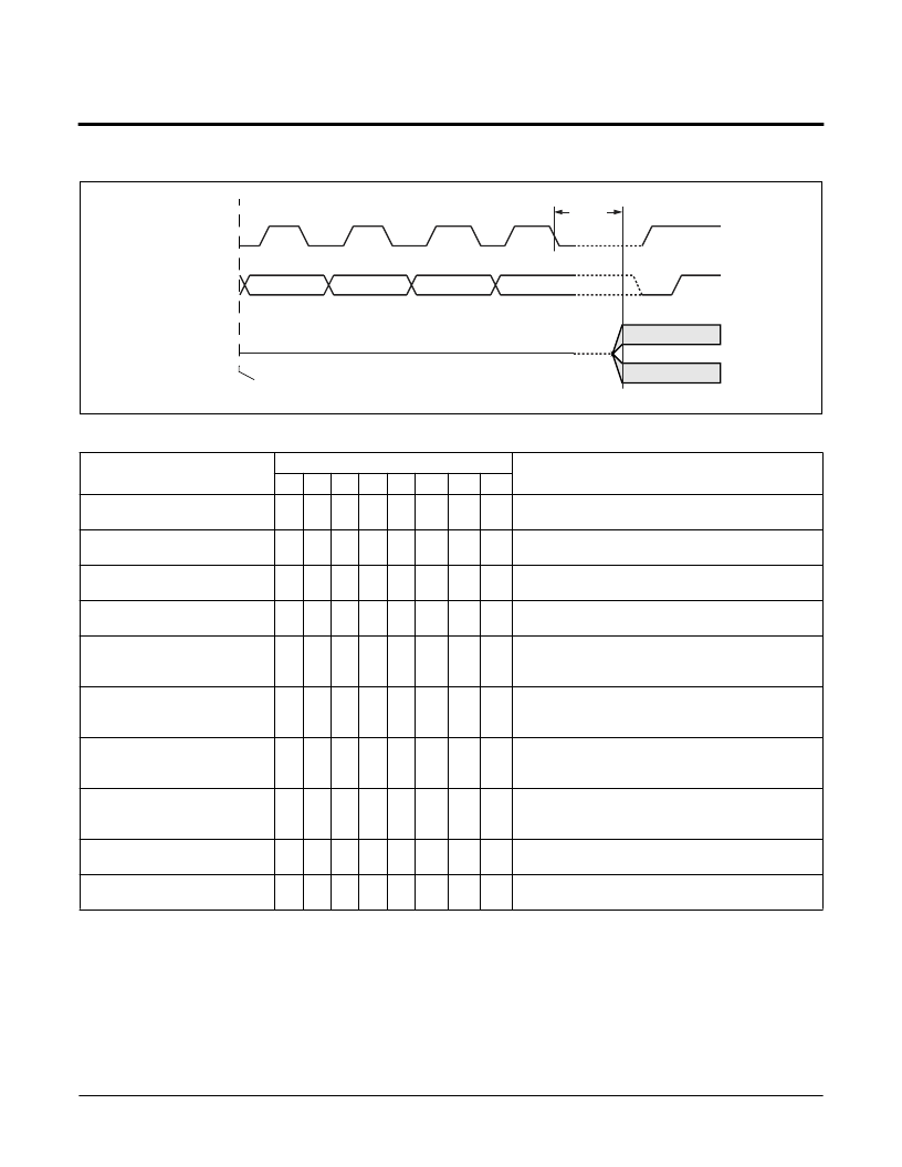
Figure 8. Increment/Decrement Timing Limits
Table 1. Instruction Set
Instruction
Instruction Set
I
1
I
0
0
1
Operation
I
3
1
I
2
0
R
1
R
0
0
P
1
P
1
P
0
P
0
Read Wiper Counter Register
0
Read the contents of the Wiper Counter Register
pointed to by P
1
-P
0
Write new value to the Wiper Counter Register
pointed to by P
1
-P
0
Read the contents of the Data Register pointed
to by P
1
-P
0
and R
1
–R
0
Write new value to the Data Register pointed to
by P
1
-P
0
and R
1
–R
0
Transfer the contents of the Data Register pointed
to by R
1
–R
0
to the Wiper Counter Register pointed
to by P
1
-P
0
Transfer the contents of the Wiper Counter
Register pointed to by P
1
-P
0
to the Register
pointed to by R
1
–R
0
Transfer the contents of the Data Registers
pointed to by R
1
–R
0
of all four pots to their
respective Wiper Counter Register
Transfer the contents of all Wiper Counter
Registers to their respective data Registers
pointed to by R
1
–R
0
of all four pots
Enable Increment/decrement of the Wiper
Counter Register pointed to by P
1
-P
0
Read the status of the internal write cycle, by
checking the WIP bit.
Write Wiper Counter Register
1
0
1
0
0
0
P
1
P
0
Read Data Register
1
0
1
1
R
1
R
0
P
1
P
0
Write Data Register
1
1
0
0
R
1
R
0
P
1
P
0
XFR Data Register to Wiper
Counter Register
1
1
0
1
R
1
R
0
P
1
P
0
XFR Wiper Counter Register
to Data Register
1
1
1
0
R
1
R
0
P
1
P
0
Global XFR Data Register to
Wiper Counter Register
0
0
0
1
R
1
R
0
0
0
Global XFR Wiper Counter
Register to Data Register
1
0
0
0
R
1
R
0
0
0
Increment/Decrement Wiper
Counter Register
Read Status (WIP bit)
0
0
1
0
0
0
P
1
P
0
0
1
0
1
0
0
0
1
SCK
SI
V
W
/R
W
INC/DEC CMD Issued
t
WRID
Voltage Out
相關(guān)PDF資料 |
PDF描述 |
|---|---|
| X9400YZ24I-2.7 | Quad Digitally Controlled Potentiometers (XDCP) |
| X9400 | RF/Microwave Capacitor; Capacitance:20pF; Capacitance Tolerance:+/- 5%; Series:MC; Capacitor Dielectric Material:Mica; Termination:SMD; Leaded Process Compatible:No; Peak Reflow Compatible (260 C):No RoHS Compliant: No |
| X9400WP24 | Digital Potentiometer |
| X9400WP24-2.7 | Digital Potentiometer |
| X9400WP24I | Digital Potentiometer |
相關(guān)代理商/技術(shù)參數(shù) |
參數(shù)描述 |
|---|---|
| X9400YZ24I-2.7 | 制造商:XICOR 制造商全稱(chēng):Xicor Inc. 功能描述:Quad Digitally Controlled Potentiometers (XDCP) |
| X9401 | 制造商:INTERSIL 制造商全稱(chēng):Intersil Corporation 功能描述:Low Noise/Low Power/SPI Bus |
| X9401_06 | 制造商:INTERSIL 制造商全稱(chēng):Intersil Corporation 功能描述:Quad, 64 Tap, Digitally Controlled Potentiometer |
| X9401_09 | 制造商:INTERSIL 制造商全稱(chēng):Intersil Corporation 功能描述:Quad, 64 Tap, Digitally Controlled Potentiometer (XDCP?) |
| X94012011-01 | 功能描述:以太網(wǎng)模塊 XPress-Pro SW 94012F 8-Port 10/100TX RoHS:否 制造商:Lantronix 產(chǎn)品:Device Servers 數(shù)據(jù)速率:300 bps to 921.6 kbps, 10 Mbps, 100 Mbps 接口類(lèi)型:Ethernet, Serial 工作電源電壓:5 V to 15 V 工作電源電流:133 mA to 400 mA 最大工作溫度:+ 70 C |
發(fā)布緊急采購(gòu),3分鐘左右您將得到回復(fù)。