- 您現(xiàn)在的位置:買賣IC網(wǎng) > PDF目錄371276 > X88C64PM E2 Micro-Peripheral PDF資料下載
參數(shù)資料
| 型號(hào): | X88C64PM |
| 英文描述: | E2 Micro-Peripheral |
| 中文描述: | E2微型外設(shè) |
| 文件頁(yè)數(shù): | 5/14頁(yè) |
| 文件大小: | 71K |
| 代理商: | X88C64PM |
第1頁(yè)第2頁(yè)第3頁(yè)第4頁(yè)當(dāng)前第5頁(yè)第6頁(yè)第7頁(yè)第8頁(yè)第9頁(yè)第10頁(yè)第11頁(yè)第12頁(yè)第13頁(yè)第14頁(yè)
X88C64
5
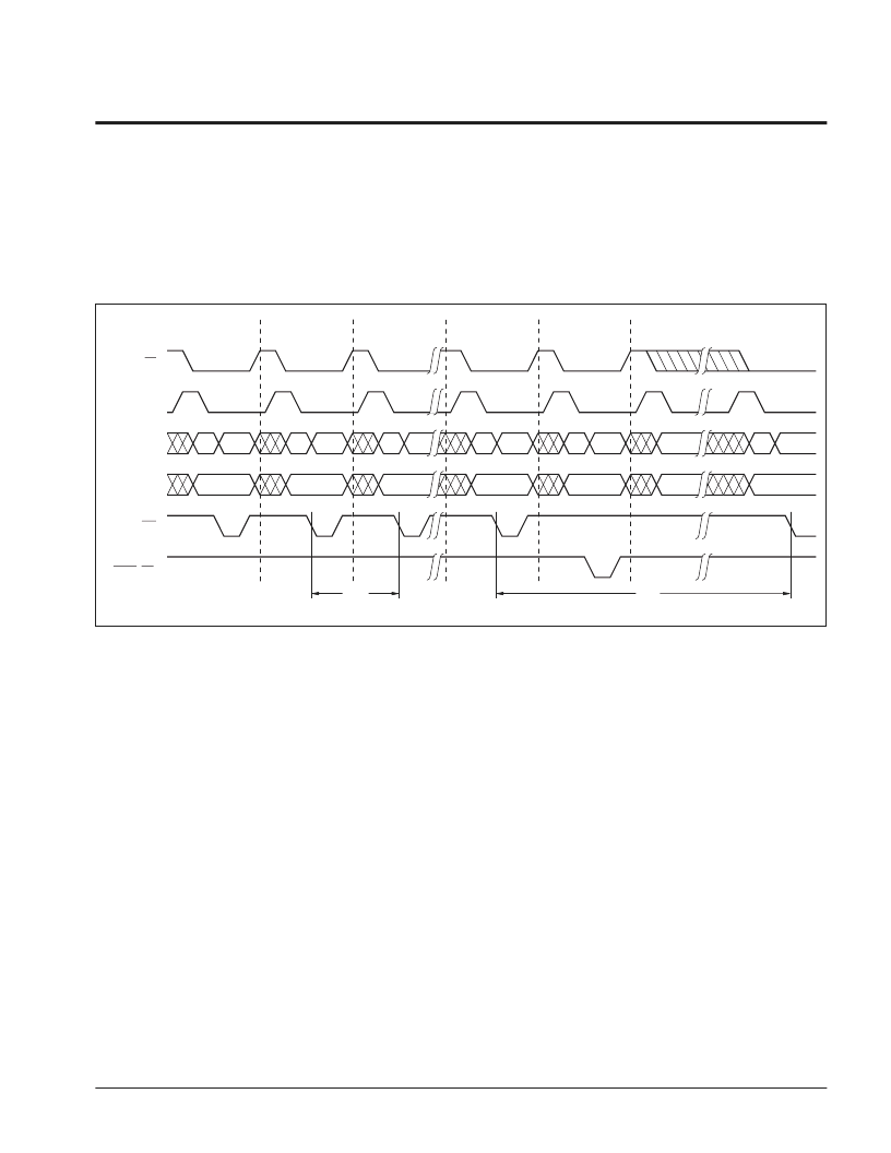
Page Write Timing Sequence for
WR
Controlled Operation
Notes:
(1) For each successive write within a page write cycle A
5
–A
12
must be the same.
(2) Although it is not illustrated, the microcontroller may interleave read operations between the individual byte writes within the page
write operation. Two responses are possible:
a. Reading from the same plane being written (A
12
of Read = A
12
of Write) is effectively a Toggle Bit Polling operation.
b. Reading from the opposite plane being written (A
12
of Read
≠
A
12
of Write) true data will be returned, facilitating the use of a
single memory component as both program and data storage.
PAGE WRITE OPERATION
Regardless of the microcontroller employed, the X88C64
supports page mode write operations. This allows the
microcontroller to write from one to thirty-two bytes of
data to the X88C64. Each individual write within a page
write operation must conform to the byte write timing
requirements. The falling edge of
WR
starts a timer
delaying the internal programming cycle 100
μ
s. There-
fore, each successive write operation must begin within
100
μ
s of the last byte written. The following waveforms
illustrate the sequence and timing requirements.
3867 FHD F08
tBLC
CE
ALE
A/D0–A/D7
A8–A12
WR
PSEN(RD)
AIN
DIN
A12=n
OPERATION
BYTE 0
BYTE 1
BYTE 2
LAST BYTE
READ (1)(2)
AFTER tWC READY FOR
NEXT WRITE OPERATION
tWC
AIN
DIN
A12=n
AIN
DIN
A12=n
AIN
DIN
A12=n
AIN
DOUT
A12=x
AIN
ADDR
AIN
Next Address
相關(guān)PDF資料 |
PDF描述 |
|---|---|
| X88C64PMB | E2 Micro-Peripheral |
| X88C64SI | E2 Micro-Peripheral |
| X88C64SM | E2 Micro-Peripheral |
| X88C64SMB | E2 Micro-Peripheral |
| X88C64S | E2 Micro-Peripheral |
相關(guān)代理商/技術(shù)參數(shù) |
參數(shù)描述 |
|---|---|
| X88C64PMB | 制造商:XICOR 制造商全稱:Xicor Inc. 功能描述:E2 Micro-Peripheral |
| X88C64S | 制造商:XICOR 制造商全稱:Xicor Inc. 功能描述:E2 Micro-Peripheral |
| X88C64SI | 制造商:XICOR 制造商全稱:Xicor Inc. 功能描述:E2 Micro-Peripheral |
| X88C64SM | 制造商:XICOR 制造商全稱:Xicor Inc. 功能描述:E2 Micro-Peripheral |
| X88C64SMB | 制造商:XICOR 制造商全稱:Xicor Inc. 功能描述:E2 Micro-Peripheral |
發(fā)布緊急采購(gòu),3分鐘左右您將得到回復(fù)。