- 您現(xiàn)在的位置:買賣IC網(wǎng) > PDF目錄371276 > X88257JM E2 Micro-Peripheral PDF資料下載
參數(shù)資料
| 型號: | X88257JM |
| 英文描述: | E2 Micro-Peripheral |
| 中文描述: | E2微型外設 |
| 文件頁數(shù): | 3/15頁 |
| 文件大小: | 70K |
| 代理商: | X88257JM |
X88257
3
PRINCIPLES OF OPERATION
The X88257 is a highly integrated peripheral device for
a wide variety of single-chip microcontrollers. The X88257
provides 32K-bytes of 5V E
2
PROM which can be used
either for program storage, data storage or a combina-
tion of both, in systems based upon Harvard (80XX)
architectures. The X88257 incorporates the interface
circuitry normally needed to decode the control signals
and demultiplex the address/data bus to provide a
“seamless” interface.
The interface inputs on the X88257 are configured such
that it is possible to directly connect them to the proper
interface signals of the appropriate single-chip micro-
controller. In the Harvard type system, the reading of
data from the chip is controlled either by the
PSEN
or the
RD
signal, which essentially maps the X88257 into both
the Program and the Data Memory address map.
The X88257 also features the industry standard 5V
E
2
PROM characteristics such as byte or page mode
write and Toggle Bit Polling.
DEVICE OPERATION
Modes—Mixed Program/Data Memory
By properly assigning the address spaces, a single
X88257 can be used as both the program and data
memory. This would be accomplished by connecting all
the 8051 control outputs to the corresponding inputs of
the X88257.
Program Memory Mode
This mode of operation is read-only. The
PSEN
and
ALE
inputs of the X88257 are tied directly to the
PSEN
and
ALE outputs of the microcontroller. The
RD
and
WR
inputs are tied HIGH.
When ALE is HIGH, the A/D
0
–A/D
7
and A
8
–A
14
ad-
dresses flow into the device. The addresses, both low-
and high-order, are latched when ALE transitions LOW
(V
IL
).
PSEN
will then go LOW and after t
PLDV
; Valid data
is presented on the A/D
0
–A/D
7
pins.
CE
must be LOW
during the entire operation.
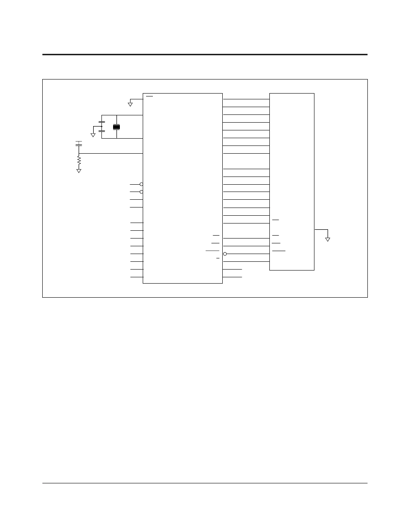
TYPICAL APPLICATION
6509 ILL F03.3
P0.0
P0.1
P0.2
P0.3
P0.4
P0.5
P0.6
P0.7
P2.0
P2.1
P2.2
P2.3
P2.4
P2.5
P2.6
P2.7
RD
WR
PSEN
ALE/P
TXD
RXD
39
38
37
36
35
34
33
32
5
31
19
18
9
EA/VP
X1
U
X2
RESET
CE
21
22
23
24
25
26
27
28
11
12
12
15
16
17
18
19
25
24
21
23
2
26
1
20
1
2
3
4
5
6
7
8
12
13
14
15
INT0
INT1
T0
T1
P1.0
P1.1
P1.2
P1.3
P1.4
P1.5
P1.6
P1.7
A/D0
A/D1
A/D2
A/D3
A/D4
A/D5
A/D6
A/D7
A8
A9
A10
A11
A12
A13
A14
CE
RD
WR
PSEN
ALE
17
16
30
11
10
8051
22
27
4
3
29
X88257
相關PDF資料 |
PDF描述 |
|---|---|
| X88257P | E2 Micro-Peripheral |
| X88257PI | E2 Micro-Peripheral |
| X88257PM | E2 Micro-Peripheral |
| X88257S | E2 Micro-Peripheral |
| X88257SI | E2 Micro-Peripheral |
相關代理商/技術參數(shù) |
參數(shù)描述 |
|---|---|
| X88257P | 制造商:XICOR 制造商全稱:Xicor Inc. 功能描述:E2 Micro-Peripheral |
| X88257PI | 制造商:XICOR 制造商全稱:Xicor Inc. 功能描述:E2 Micro-Peripheral |
| X88257PM | 制造商:XICOR 制造商全稱:Xicor Inc. 功能描述:E2 Micro-Peripheral |
| X88257S | 制造商:XICOR 制造商全稱:Xicor Inc. 功能描述:E2 Micro-Peripheral |
| X88257SI | 制造商:XICOR 制造商全稱:Xicor Inc. 功能描述:E2 Micro-Peripheral |
發(fā)布緊急采購,3分鐘左右您將得到回復。