- 您現(xiàn)在的位置:買賣IC網(wǎng) > PDF目錄371276 > X88257J E2 Micro-Peripheral PDF資料下載
參數(shù)資料
| 型號: | X88257J |
| 英文描述: | E2 Micro-Peripheral |
| 中文描述: | E2微型外設(shè) |
| 文件頁數(shù): | 4/15頁 |
| 文件大?。?/td> | 70K |
| 代理商: | X88257J |
X88257
4
MODE SELECTION
CE
PSEN
RD
WR
Mode
I/O
Power
V
CC
HIGH
LOW
LOW
LOW
X
X
X
X
X
X
Standby
Standby
Read
Read
Write
High Z
High Z
D
OUT
D
OUT
D
IN
Standby (CMOS)
Standby (TTL)
Active
Active
Active
LOW
HIGH
HIGH
HIGH
LOW
HIGH
HIGH
HIGH
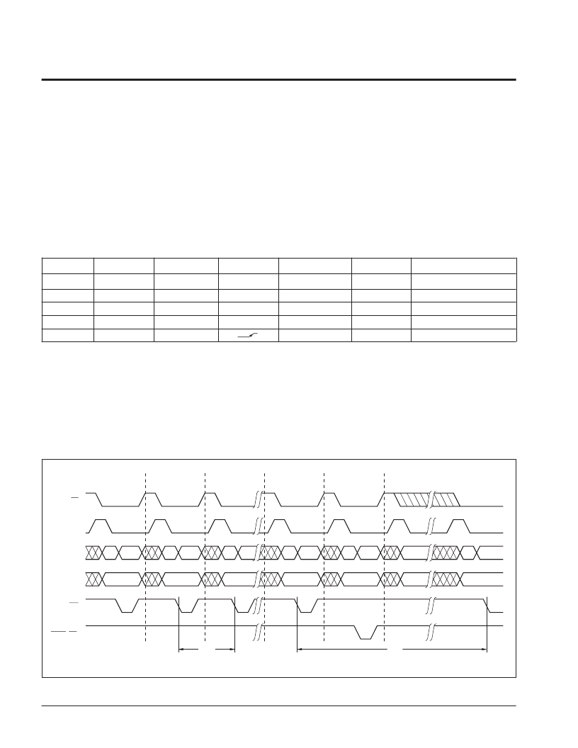
Page Write Timing Sequence for
WR
Controlled Operation
Notes:
(1) For each successive write within a page write cycle A
7
–A
14
must be the same.
PAGE WRITE OPERATION
Regardless of the microcontroller employed, the X88257
supports page mode write operations. This allows the
microcontroller to write from 1 to 128 bytes of data to the
X88257. Each individual write within a page write opera-
tion must conform to the byte write timing requirements.
The falling edge of
WR
starts a timer delaying the
internal programming cycle 100
μ
s. Therefore, each
successive write operation must begin within 100
μ
s of
the last byte written. The following waveforms illustrate
the sequence and timing requirements.
6509 PGM T02
tBLC
CE
ALE
A/D0–A/D7
A8–A14
WR
PSEN(RD)
AIN
DIN
An
OPERATION
BYTE 0
BYTE 1
BYTE 2
LAST BYTE
READ (1)(2)
AFTER tWC READY FOR
NEXT WRITE OPERATION
tWC
6509 ILL F08.1
AIN
DIN
An
AIN
DIN
An
AIN
DIN
An
AIN
DOUT
An
AIN
ADDR
AIN
Next Address
DATA MEMORY MODE
This mode of operation allows both read and write
functions. The
PSEN
input is tied to V
IH
or to V
CC
through a pull-up resistor. The ALE,
RD
, and
WR
inputs
are tied directly to the microcontroller ALE,
RD
, and
WR
outputs.
Read
This operation is quite similar to the program memory
read. A HIGH to LOW transition on ALE latches the
addresses and the data will be output on the AD pins
after
RD
goes LOW (t
RLDV
).
Write
A write is performed by latching the addresses on the
falling edge of ALE. Then
WR
is strobed LOW followed
by valid data being presented at the A/D
0
–A/D
7
pins.
The data will be latched into the X88257 on the rising
edge of
WR
. To write to the X88257, a three-byte
command sequence must precede the byte(s) being
written. (See Software Data Protection.)
相關(guān)PDF資料 |
PDF描述 |
|---|---|
| X88257JI | E2 Micro-Peripheral |
| X88257JM | E2 Micro-Peripheral |
| X88257P | E2 Micro-Peripheral |
| X88257PI | E2 Micro-Peripheral |
| X88257PM | E2 Micro-Peripheral |
相關(guān)代理商/技術(shù)參數(shù) |
參數(shù)描述 |
|---|---|
| X88257JI | 制造商:XICOR 制造商全稱:Xicor Inc. 功能描述:E2 Micro-Peripheral |
| X88257JM | 制造商:XICOR 制造商全稱:Xicor Inc. 功能描述:E2 Micro-Peripheral |
| X88257P | 制造商:XICOR 制造商全稱:Xicor Inc. 功能描述:E2 Micro-Peripheral |
| X88257PI | 制造商:XICOR 制造商全稱:Xicor Inc. 功能描述:E2 Micro-Peripheral |
| X88257PM | 制造商:XICOR 制造商全稱:Xicor Inc. 功能描述:E2 Micro-Peripheral |
發(fā)布緊急采購,3分鐘左右您將得到回復(fù)。