- 您現(xiàn)在的位置:買賣IC網(wǎng) > PDF目錄371276 > X86C64S E2 Micro-Peripheral PDF資料下載
參數(shù)資料
| 型號: | X86C64S |
| 英文描述: | E2 Micro-Peripheral |
| 中文描述: | E2微型外設 |
| 文件頁數(shù): | 7/12頁 |
| 文件大?。?/td> | 62K |
| 代理商: | X86C64S |
X86C64
7
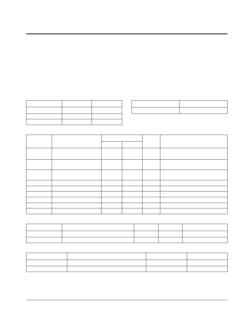
ABSOLUTE MAXIMUM RATINGS*
Temperature Under Bias
X86C64........................................ –10
°
C to +85
°
C
X86C64I..................................... –65
°
C to +135
°
C
Storage Temperature ....................... –65
°
C to +150
°
C
Voltage on any Pin with
Respect to V
SS
............................... –1.0V to +7V
D.C. Output Current ............................................5 mA
Lead Temperature
(Soldering, 10 Seconds) ............................. 300
°
C
*COMMENT
Stresses above those listed under “Absolute Maximum
Ratings” may cause permanent damage to the device.
This is a stress rating only and the functional operation of
the device at these or any other conditions above those
indicated in the operational sections of this specification
is not implied. Exposure to absolute maximum rating
conditions for extended periods may affect device reli-
ability.
RECOMMENDED OPERATING CONDITIONS
Temperature
Min.
0
°
C
–40
°
C
–55
°
C
Max.
70
°
C
+85
°
C
+125
°
C
3819 PGM T02
Commercial
Industrial
Military
Supply Voltage
Limits
5V
±
10%
X86C64
3819 PGM T03
D.C. OPERATING CHARACTERISTICS
(Over recommended operating conditions unless otherwise specified.)
Limits
Symbol
Parameter
Min.
Max.
Units
Test Conditions
I
CC
V
CC
Current (Active)
60
mA
CE = V
IL
, All I/O’s = Open,
Other Inputs = V
CC
,
AS
= V
IL
CE = V
SS
,
All I/O’s = Open,Other
Inputs = V
CC
– 0.3V
CE = V
IH
, All I/O’s = Open, Other
Inputs = V
IH
V
IN
CC
V
OUT
= GND to V
CC
,
DS
= V
IH
I
SB1(CMOS)
V
CC
Current (Standby)
500
μ
A
I
SB2(TTL)
V
CC
Current (Standby)
6
mA
I
LI
I
LO
V
lL(1)
V
IH(1)
V
OL
V
OH
Input Leakage Current
Output Leakage Current
Input Low Voltage
Input High Voltage
Output Low Voltage
Output High Voltage
10
10
0.8
μ
A
μ
A
V
V
V
V
–1.0
2.0
V
CC
+ 0.5
0.4
I
OL
= 2.1 mA
I
OH
= –400
μ
A
2.4
3819 PGM T04
CAPACITANCE
T
A
= 25
°
C, F = 1.0MHZ, V
CC
= 5V
Symbol
Test
Max.
Units
Conditions
C
I/O(2)
C
IN(2)
Input/Output Capacitance
Input Capacitance
10
6
pF
pF
V
I/O
= 0V
V
IN
= 0V
3819 PGM T05
POWER-UP TIMING
Symbol
Parameter
Max.
Units
t
PUR(2)
t
PUW(2)
Power-Up to Read
Power-Up to Write
1
5
ms
ms
3819 PGM T06
Notes:
(1) V
IL
MIN and V
IH
MAX are for reference only and are not tested.
(2) This parameter is periodically sampled and not 100% tested.
相關PDF資料 |
PDF描述 |
|---|---|
| X86C64SI | E2 Micro-Peripheral |
| X86C64SM | E2 Micro-Peripheral |
| X88257 | E2 Micro-Peripheral |
| X88257J | E2 Micro-Peripheral |
| X88257JI | E2 Micro-Peripheral |
相關代理商/技術參數(shù) |
參數(shù)描述 |
|---|---|
| X86C64SI | 制造商:XICOR 制造商全稱:Xicor Inc. 功能描述:E2 Micro-Peripheral |
| X86C64SM | 制造商:XICOR 制造商全稱:Xicor Inc. 功能描述:E2 Micro-Peripheral |
| X8701-10 | 制造商:Cooper Crouse-Hinds 功能描述: |
| X8701-3 | 制造商:Cooper Crouse-Hinds 功能描述: |
| X87104121 | 制造商:n/a 功能描述:SOCKET 4PIN BULK |
發(fā)布緊急采購,3分鐘左右您將得到回復。