- 您現(xiàn)在的位置:買賣IC網(wǎng) > PDF目錄300104 > WG1602B-Y-JCS (DB Lectro Inc.) WP1602B-Y-JCS PDF資料下載
參數(shù)資料
| 型號: | WG1602B-Y-JCS |
| 廠商: | DB Lectro Inc. |
| 英文描述: | WP1602B-Y-JCS |
| 中文描述: | WP1602B - Y型參聯(lián)會 |
| 文件頁數(shù): | 3/17頁 |
| 文件大小: | 336K |
| 代理商: | WG1602B-Y-JCS |
第 13 頁,共 19 頁
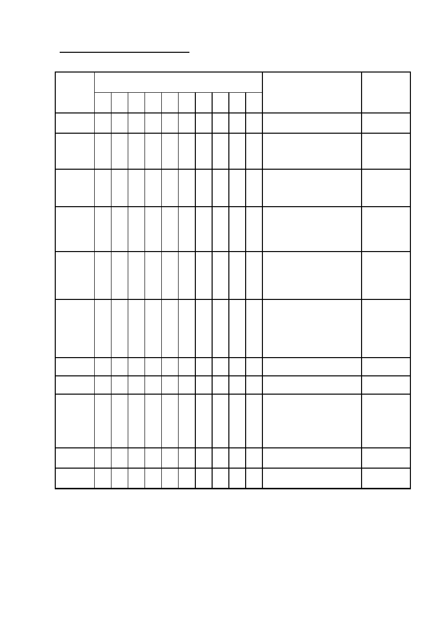
11.Instruction Table
Instruction Code
Instruction
RS R/W DB7 DB6 DB5 DB4 DB3 DB2 DB1 DB0
Description
Execution time
(fosc=270Khz)
Clear Display
0
1
Write “00H” to DDRAM and set
DDRAM address to “00H” from AC
1.52ms
Return Home
0
1
-
Set DDRAM address to “00H” from AC
and return cursor to its original position
if shifted. The contents of DDRAM are
not changed.
1.52ms
Entry Mode
Set
0
1
I/D
SH
Assign cursor moving direction and
enable the shift of entire display.
I/D=1:Increment
;0: Decrement
SH=1:Display shift on
37
μ s
Display
ON/OFF
Control
0
1
D
C
B
Set display (D), cursor (C), and blinking
of cursor (B) on/off control bit.
D=1:Display on
C=1:Cursor display on
B=1:Cursor blink on
37
μ s
Cursor or
Display Shift
0
1
S/C R/L
-
Set cursor moving and display shift
control bit, and the direction, without
changing of DDRAM data.
S/C=1:Shift display
;0:Move cursor
R/L=1:Shift right
;0:Shift leftf
37
μ s
Function Set
0
1
DL
N
F
-
Set interface data length (DL)
DL=1:8-bit
;0:4-bit
Set numbers of display lines(N)
N=1:Dual line
;0:Single line
Set display font type (F)
F=1:5x10 dots
;0:5x8dots
37
μ s
Set CGRAM
Address
0
1
AC5 AC4 AC3 AC2 AC1 AC0 Set CGRAM address in address counter.
37
μ s
Set DDRAM
Address
0
1
AC6 AC5 AC4 AC3 AC2 AC1 AC0 Set DDRAM address in address counter.
37
μ s
Read Busy
Flag and
Address
0
1
BF AC6 AC5 AC4 AC3 AC2 AC1 AC0
Whether during internal operation or not
can be known by reading BF. The
contents of address counter can also be
read.
BF=1:Internal operation
BF=0:Ready for instruction
0
μ s
Write Data to
RAM
1
0
D7
D6
D5
D4
D3
D2
D1
D0
Write data into internal RAM
(DDRAM/CGRAM).
37
μ s
Read Data
from RAM
1
D7
D6
D5
D4
D3
D2
D1
D0
Read data from internal RAM
(DDRAM/CGRAM).
37
μ s
* ”-”:don’t care
相關PDF資料 |
PDF描述 |
|---|---|
| WG160PRW40 | TWO PART BOARD CONNECTOR |
| WG2002A-Y-JCS | WP2002A-Y-JCS |
| WG92SAW24SY-1 | 92 CONTACT(S), FEMALE, STRAIGHT TWO PART BOARD CONNECTOR, WIRE WRAP, RECEPTACLE |
| WGA122PR7 | TWO PART BOARD CONNECTOR |
| WGA122PR9 | TWO PART BOARD CONNECTOR |
相關代理商/技術參數(shù) |
參數(shù)描述 |
|---|---|
| WG160SACSY65 | 制造商:Airborn Inc 功能描述: |
| WG16A | 制造商:NSC 制造商全稱:National Semiconductor 功能描述:CERPACK |
| WG18008RXX | 制造商:未知廠家 制造商全稱:未知廠家 功能描述:GATE TURN THYRISTORS |
| WG18012R | 制造商:未知廠家 制造商全稱:未知廠家 功能描述:THYRISTOR|GTO|TO-200AE |
| WG18014R | 制造商:未知廠家 制造商全稱:未知廠家 功能描述:THYRISTOR|GTO|TO-200AE |
發(fā)布緊急采購,3分鐘左右您將得到回復。