- 您現(xiàn)在的位置:買賣IC網(wǎng) > PDF目錄231493 > WF2M32-120G2UC5 2M X 32 FLASH 5V PROM MODULE, 120 ns, CQFP68 PDF資料下載
參數(shù)資料
| 型號: | WF2M32-120G2UC5 |
| 元件分類: | PROM |
| 英文描述: | 2M X 32 FLASH 5V PROM MODULE, 120 ns, CQFP68 |
| 封裝: | 22.40 MM, CERAMIC, QFP-68 |
| 文件頁數(shù): | 9/14頁 |
| 文件大小: | 174K |
| 代理商: | WF2M32-120G2UC5 |
4
White Electronic Designs Corporation Phoenix, AZ (602) 437-1520
WF2M32-XXX5
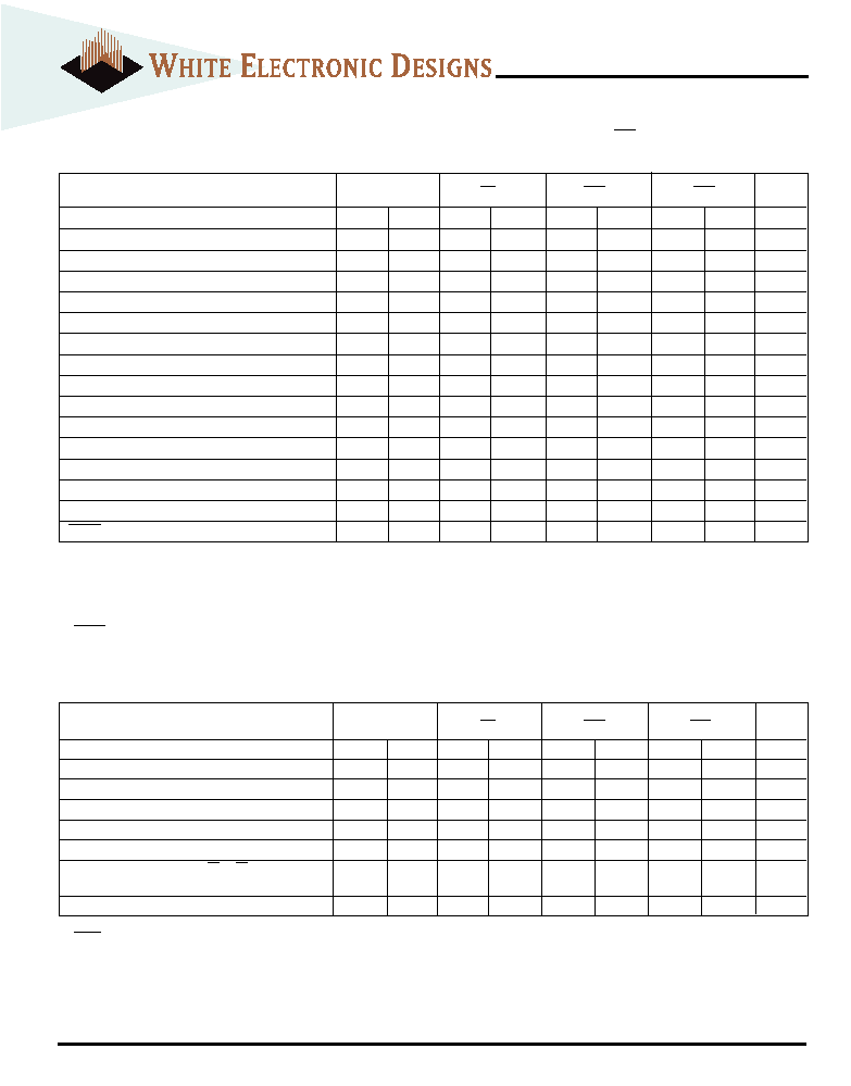
AC CHARACTERISTICS – WRITE/ERASE/PROGRAM OPERATIONS - WE CONTROLLED
(VCC = 5.0V, TA = -55
°C to +125°C)
Parameter
Symbol
-90
-120
-150
Unit
Min
Max
Min
Max
Min
Max
Write Cycle Time
tAVAV
tWC
90
120
150
ns
Chip Select Setup Time
tELWL
tCS
00
0
ns
Write Enable Pulse Width
tWLWH
tWP
45
50
ns
Address Setup Time
tAVWL
tAS
00
0
ns
Data Setup Time
tDVWH
tDS
45
50
ns
Data Hold Time
tWHDX
tDH
00
0
ns
Address Hold Time
tWLAX
tAH
45
50
ns
Write Enable Pulse Width High
tWHWL
tWPH
20
ns
Duration of Byte Programming Operation (1)
tWHWH1
300
s
Sector Erase (2)
tWHWH2
15
sec
Read Recovery Time before Write
tGHWL
00
0
s
VCC Setup Time
tVCS
50
s
Chip Programming Time
44
sec
Chip Erase Time (3)
256
sec
Output Enable Hold Time (4)
tOEH
10
ns
RESET Pulse Width (5)
tRP
500
ns
NOTES:
1. Typical value for tWHWH1 is 7
s.
2. Typical value for tWHWH2 is 1sec.
3. Typical value for Chip Erase Time is 32sec.
4. For Toggle and Data Polling.
5. RESET internally tied to Vcc for the default pin configuration in the HIP package.
AC CHARACTERISTICS – READ-ONLY OPERATIONS
(VCC = 5.0V, TA = -55
°C to +125°C)
Parameter
Symbol
-90
-120
-150
Unit
Min
Max
Min
Max
Min
Max
Read Cycle Time
tAVAV
tRC
90
120
150
ns
Address Access Time
tAVQV
tACC
90
120
150
ns
Chip Select Access Time
tELQV
tCE
90
120
150
ns
Output Enable to Output Valid
tGLQV
tOE
40
50
55
ns
Chip Select High to Output High Z (1)
tEHQZ
tDF
20
30
35
ns
Output Enable High to Output High Z (1)
tGHQZ
tDF
20
30
35
ns
Output Hold from Addresses, CS or OE Change,
tAXQX
tOH
00
0
ns
whichever is First
RST Low to Read Mode (1,2)
tReady
20
s
1. Guaranteed by design, not tested.
2. RESET internally tied to Vcc for the default pin configuration in the HIP package.
發(fā)布緊急采購,3分鐘左右您將得到回復(fù)。