- 您現(xiàn)在的位置:買賣IC網(wǎng) > PDF目錄202705 > VT-701-EAJ-106D-25M0000000 (VECTRON INTERNATIONAL) TCVCXO, CLOCK, 25 MHz, CMOS OUTPUT PDF資料下載
參數(shù)資料
| 型號(hào): | VT-701-EAJ-106D-25M0000000 |
| 廠商: | VECTRON INTERNATIONAL |
| 元件分類: | TCVCXO, clock |
| 英文描述: | TCVCXO, CLOCK, 25 MHz, CMOS OUTPUT |
| 封裝: | ROHS COMPLIANT, HERMETIC SEALED. CERAMIC, SMD, 10 PIN |
| 文件頁(yè)數(shù): | 2/5頁(yè) |
| 文件大小: | 0K |
| 代理商: | VT-701-EAJ-106D-25M0000000 |
Vectron International 267 Lowell Road, Hudson, NH 03051 Tel: 1-88-VECTRON-1 http://www.vectron.com
Page2
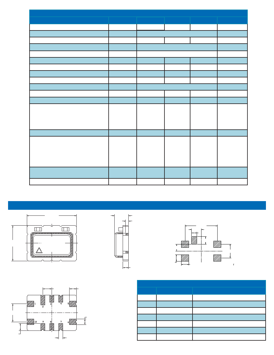
Table 1. Electrical Performance
Parameter
Symbol
Min.
Typ
Max
Units
Output Frequency
f
O
527
MHz
Supply Voltage1, Ordering Option
V
DD
+3.3 or +5.0
Vdc
Supply Current
I
DD
10
mA
Operating Temperature, Ordering Option
T
OP
0/55, -10/60, -20/70, -30/80, -40/85
°C
Stability Over T
OP
, Ordering Option
±0.5, ±1.0, ±.5, ±2.0, ±2.5, ±3.0, ±4.0, ±5.0
ppm
Initial Accuracy, “No Adjust” Option
±1.0
ppm
Power Supply Stability
±0.3
ppm
Load Stability
±0.2
ppm
Aging
±1.0
ppm/yr
Pull Range, ordering option
TPR
±5, ±8, ±10, ±12
ppm
Control Voltage to reach Pull Range
0.5
2.5
V
Control Voltage Impedance
1
Mohm
Output Level2
Output Logic High
Output Logic Low
Output Logic High Drive
Output Logic Low Drive
V
OH
V
OL
I
OH
I
OL
0.8*V
DD
4
0.1*V
DD
-4
V
mA
Output Load
15
pF
Phase Noise, 10.000MHz
10Hz
100Hz
1kHz
10kHz
100kHz
-92
-116
-137
-149
-154
dBc/Hz
Enable Disable3 , Output Enbaled
Output Disabled
V
IH
V
IL
0.3*
VDD
0.7*V
DD
Start Up Time
2ms
1. The V-701 power supply pin should be filtered, eg, a 0.1 and 0.01uf capacitor
2. The Output is DC coupled
3. Output is Enabled if E/D is left open
Table 2. Pinout
Pin #
Symbol
Function
1V
C
TCXO Control Voltage or Ground
2,3,4
NC
Make No Connection
5
GND
Electrical and Lid Ground
6f
O
Output Frequency
7,8
NC
Make No Connection
9
E/D
Enable Disable
10
V
DD
Supply Voltage
Pad Layout mm
Outline Drawing
Recommended Pad Layout
1.4
1.2
1.4
6.0
1.8
1.4 1.0
1.3
2.54
0.4±0.1
Dimensions in mm
7.0±01
5.0±0.1
1.27±0.1
1.0±0.1
0.8±0.1
0.6±0.1
2.54±0.1
2.0 max
0.8 typ
1.0±0.1
FREQUENCY
Date Code
相關(guān)PDF資料 |
PDF描述 |
|---|---|
| VT-701-EAJ-156C-12M8000000 | TCVCXO, CLOCK, 12.8 MHz, CMOS OUTPUT |
| VT-701-EAR-306D-12M5000000 | TCVCXO, CLOCK, 12.5 MHz, CMOS OUTPUT |
| VT-701-EAR-356C-19M2000000 | TCVCXO, CLOCK, 19.2 MHz, CMOS OUTPUT |
| VT-701-DAG-206D-20M0000000 | TCVCXO, CLOCK, 20 MHz, CMOS OUTPUT |
| VT-701-DAG-256A-12M8000000 | TCVCXO, CLOCK, 12.8 MHz, CMOS OUTPUT |
相關(guān)代理商/技術(shù)參數(shù) |
參數(shù)描述 |
|---|---|
| VT7202 | 制造商:未知廠家 制造商全稱:未知廠家 功能描述:1,024 X 9 FIFO MEMORY |
| VT7203 | 制造商:未知廠家 制造商全稱:未知廠家 功能描述:2,048 X 9 FIFO MEMORY |
| VT7203-20 | 制造商:未知廠家 制造商全稱:未知廠家 功能描述:2,048 X 9 FIFO MEMORY |
| VT7203-35 | 制造商:未知廠家 制造商全稱:未知廠家 功能描述:2,048 X 9 FIFO MEMORY |
| VT7203-50 | 制造商:未知廠家 制造商全稱:未知廠家 功能描述:2,048 X 9 FIFO MEMORY |
發(fā)布緊急采購(gòu),3分鐘左右您將得到回復(fù)。