- 您現(xiàn)在的位置:買賣IC網(wǎng) > PDF目錄359431 > VSC8113QB2 (VITESSE SEMICONDUCTOR CORP) Modular Connector; No. of Contacts:8; Approval Categories:FCC part 68, Subpart F, IEC-603-7 compliant; Meet ITA/EIA requirements; UL94V-0 fire-retardant rated; Body Material:Fire-Retardant Plastic; Color:Green RoHS Compliant: Yes PDF資料下載
參數(shù)資料
| 型號(hào): | VSC8113QB2 |
| 廠商: | VITESSE SEMICONDUCTOR CORP |
| 元件分類: | 數(shù)字傳輸電路 |
| 英文描述: | Modular Connector; No. of Contacts:8; Approval Categories:FCC part 68, Subpart F, IEC-603-7 compliant; Meet ITA/EIA requirements; UL94V-0 fire-retardant rated; Body Material:Fire-Retardant Plastic; Color:Green RoHS Compliant: Yes |
| 中文描述: | TRANSCEIVER, PQFP100 |
| 封裝: | 14 X 20 MM, 2.70 MM HEIGHT, PLASTIC, QFP-100 |
| 文件頁(yè)數(shù): | 24/28頁(yè) |
| 文件大小: | 484K |
| 代理商: | VSC8113QB2 |
第1頁(yè)第2頁(yè)第3頁(yè)第4頁(yè)第5頁(yè)第6頁(yè)第7頁(yè)第8頁(yè)第9頁(yè)第10頁(yè)第11頁(yè)第12頁(yè)第13頁(yè)第14頁(yè)第15頁(yè)第16頁(yè)第17頁(yè)第18頁(yè)第19頁(yè)第20頁(yè)第21頁(yè)第22頁(yè)第23頁(yè)當(dāng)前第24頁(yè)第25頁(yè)第26頁(yè)第27頁(yè)第28頁(yè)
VITESSE
Data Sheet
VSC8113
ATM/SONET/SDH 622 Mb/s Transceiver Mux/Demux
with Integrated Clock Generation and Clock Recovery
Page 24
VITESSE
SEMICONDUCTOR CORPORATION
741 Calle Plano, Camarillo, CA 93012 805/388-3700 FAX: 805/987-5896
G52154-0, Rev 4.2
3/19/99
Application Notes
Interconnecting the Byte Clocks (TXLSCKOUT and TXLSCKIN)
The byte clock (TXLSCKOUT and TXLSCKIN) on the VSC8113 has been brought off-chip to allow as
much flexibility in system-level clocking schemes as possible. Since the byte clock (TXLSCKOUT) clocks both
the VSC8113 and the UNI devices, it is important to pay close attention to the routing of this signal. The UNI
device in general is a CMOS part which can have very wide spreads in timing (1-11ns clock in to parallel data
out for the PM5355), which utilizes most of the 12.86ns period (at 78MHz), leaving little for the trace delays
and set-up times required to interconnect the 2 devices.
The VSC8113 and the UNI device should be placed as close to each other as possible to provide maximum
setup and hold time margin at the inputs of the VSC8113. Figure 12 suggests two different ways of routing the
TXLSCKOUT-to-TXLSCKIN clock trace when used in a 622 MHz mode, which ever method is used the trans-
mission line trace impedance should be no lower than 75 ohms.
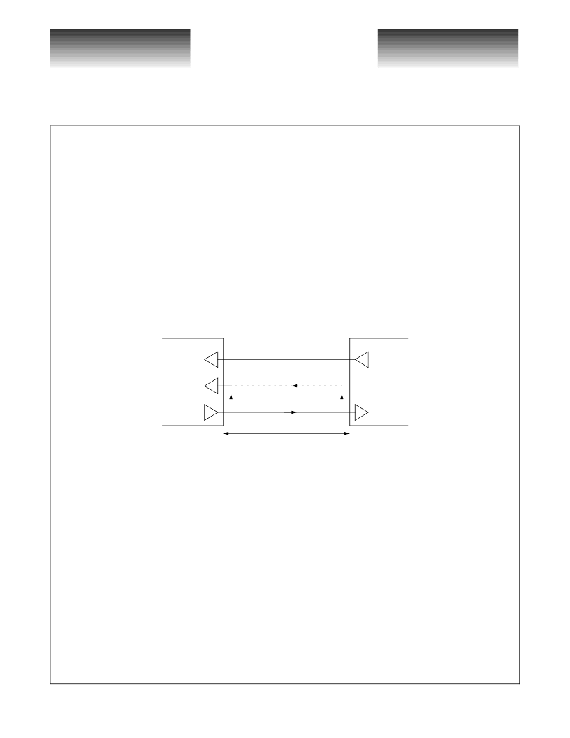
Figure 12: Interconnecting the Byte Clocks
(1) TXLSCKOUT and TXLSCKIN are tied together at the pins of the VSC8113. This provides a setup and
hold time margin for the TXIN input of
T
su,margin
= T
clk
- T
TCLK-POUT,max
(PM5355) - T
su,min
(VSC8113) - 2xT
trace
= 0.86ns - 2xT
trace
T
hold,margin
= T
TCLK-POUT,min
(PM5355) - T
hold,min
(VSC8113) + 2xT
trace
= 2xT
trace
(2) TXLSCKOUT is daisy chained to the UNI device and then routed back to the VSC8113 along with the
byte data. This interface provides a setup and hold time margin for the TXIN input of
T
su,margin
= T
clk
- T
TCLK-POUT,max
(PM5355) - T
su,min
(VSC8113) = 0.86ns
T
hold,margin
= T
TCLK-POUT,min
(PM5355) - T
hold,min
(VSC8113) = 0ns
Option (2) does not provide any hold time margin, while option (1) requires the one-way trace delay (T
trace
)
to be less than 0.43ns (~3 inches).
The general recommendation is to apply option (1) and place the VSC8113 and PM5355 as close to each
other as possible. If the one-way trace delay cannot be kept less than 0.43ns with a 50 pf load, daisy-chaining
(option 2) should be applied - close attention must be paid to signal routing in this case because of the lack of
hold time margin.
TXIN[7:0]
TXLSCKIN
TXLSCKOUT
PM5355
VSC8113
(1)
(2)
POUT[7:0]
TCLK
T
trace
相關(guān)PDF資料 |
PDF描述 |
|---|---|
| VSC8114 | ATM/SONET/SDH 622 Mb/s Transceiver Mux/Demux with Integrated Clock Generation and Clock Recovery |
| VSC8114QB | VGA TO VIDEO ULTIMATE PRO |
| VSC8114QB1 | VGA TO HDTV CONVERTER PLUS |
| VSC8114QB2 | COMPACT RGB SKEW COMPENSATOR |
| VSC8115YA1 | STS-12/STS-3 Multi Rate Clock and Data Recovery Unit |
相關(guān)代理商/技術(shù)參數(shù) |
參數(shù)描述 |
|---|---|
| VSC8114 | 制造商:VITESSE 制造商全稱:Vitesse Semiconductor Corporation 功能描述:ATM/SONET/SDH 622 Mb/s Transceiver Mux/Demux with Integrated Clock Generation and Clock Recovery |
| VSC8114QB | 制造商:VITESSE 制造商全稱:Vitesse Semiconductor Corporation 功能描述:ATM/SONET/SDH 622 Mb/s Transceiver Mux/Demux with Integrated Clock Generation and Clock Recovery |
| VSC8114QB1 | 制造商:VITESSE 制造商全稱:Vitesse Semiconductor Corporation 功能描述:ATM/SONET/SDH 622 Mb/s Transceiver Mux/Demux with Integrated Clock Generation and Clock Recovery |
| VSC8114QB2 | 制造商:VITESSE 制造商全稱:Vitesse Semiconductor Corporation 功能描述:ATM/SONET/SDH 622 Mb/s Transceiver Mux/Demux with Integrated Clock Generation and Clock Recovery |
| VSC8115 | 制造商:VITESSE 制造商全稱:Vitesse Semiconductor Corporation 功能描述:STS-12/STS-3 Multi Rate Clock and Data Recovery Unit |
發(fā)布緊急采購(gòu),3分鐘左右您將得到回復(fù)。