- 您現(xiàn)在的位置:買賣IC網(wǎng) > PDF目錄359388 > VM6101 (意法半導(dǎo)體) IC color light sensor PDF資料下載
參數(shù)資料
| 型號(hào): | VM6101 |
| 廠商: | 意法半導(dǎo)體 |
| 英文描述: | IC color light sensor |
| 中文描述: | 余C顏色光傳感器 |
| 文件頁數(shù): | 10/17頁 |
| 文件大?。?/td> | 159K |
| 代理商: | VM6101 |
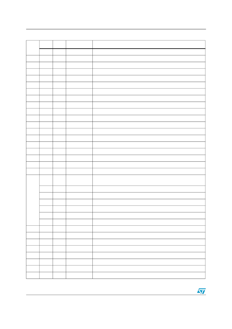
Register description
VM6101
10/17
0x05
[2:0]
0
Y_CNT3
Y channel count bits [26:24] (RO). 5 MSBs are read as zeros.
0x06
[7:0]
0
Y_CNT2
Y channel count bits [23:16] (RO)
0x07
[7:0]
0
Y_CNT1
Y channel count bits [15:8] (RO)
0x08
[7:0]
0
Y_CNT0
Y channel count bits [7:0] (RO)
0x09
[7:0]
0x01
R_STATUS
R channel status register (RO). Refer to Y Channel for description.
0x0a
[2:0]
0x00
R_CNT3
R channel count bits [26:24] (RO). 5 MSBs are read as zeros.
0x0b
[7:0]
0x00
R_CNT2
R channel count bits [23:16] (RO)
0x0c
[7:0]
0x00
R_CNT1
R channel count bits [15:8] (RO)
0x0d
[7:0]
0x00
R_CNT0
R channel count bits [7:0] (RO)
0x0e
[7:0]
0x01
G_STATUS
G channel status register (RO). Refer to Y Channel for description.
0x0f
[2:0]
0x00
G_CNT3
G channel count bits [26:24] (RO). 5 MSBs are read as zeros.
0x10
[7:0]
0x00
G_CNT2
G channel count bits [23:16] (RO)
0x11
[7:0]
0x00
G_CNT1
G channel count bits [15:8] (RO)
0x12
[7:0]
0x00
G_CNT0
G channel count bits [7:0] (RO)
0x13
[7:0]
0x01
B_STATUS
B channel status register (RO). Refer to Y Channel for description.
0x14
[2:0]
0x00
B_CNT3
B channel count bits [26:24] (RO). 5 MSBs are read as zeros.
0x15
[7:0]
0x00
B_CNT2
B channel count bits [23:16] (RO)
0x16
[7:0]
0x00
B_CNT1
B channel count bits [15:8] (RO)
0x17
[7:0]
0x00
B_CNT0
B channel count bits [7:0] (RO)
0x18
[5:0]
0x03
TH_CFG
Comparator logic configuration (RW). 2 MSBs are reserved.
Refer to
Section 2.2: Comparator logic
for programming details.
0
1
EN_LO
Enable low threshold comparator (1 = enable, 0 = disable)
1
1
POL_LO
Low threshold comparator output polarity
2
0
EN_HI
Enable high threshold comparator (1 = enable, 0 = disable)
3
0
POL_HI
High threshold comparator output polarity
4
0
INT_POL
INT pin output polarity
5
0
HYST
Enable hysteresis function
0x19
[2:0]
0x00
TH_LO3
Low threshold bits [26:24] (RW). 5 MSBs are read as zeros.
0x1a
[7:0]
0x00
TH_LO2
Low threshold bits [23:16] (RW)
0x1b
[7:0]
0x00
TH_LO1
Low threshold bits [15:8] (RW)
0x1c
[7:0]
0x08
TH_LO0
Low threshold bits [7:0] (RW)
0x1d
[2:0]
0x00
TH_HI3
High threshold bits [26:24] (RW). 5 MSBs are read as zeros.
0x1e
[7:0]
0x00
TH_HI2
High threshold bits [23:16] (RW)
0x1f
[7:0]
0x00
TH_HI1
High threshold bits [15:8] (RW)
0x20
[7:0]
0
TH_HI0
High threshold bits [7:0] (RW)
Table 3.
Register description (continued)
Addr.
Bits
Def.
Name
Description
相關(guān)PDF資料 |
PDF描述 |
|---|---|
| VM6110-4POJ | 4-Channel Disk/Tape Read/Write Circuit |
| VM6110-4TQJ | 4-Channel Disk/Tape Read/Write Circuit |
| VM6400QF | Peripheral IC |
| VM7000-2PO | Peripheral IC |
| VM700N2POL | 2-Channel Disk Read/Write Circuit |
相關(guān)代理商/技術(shù)參數(shù) |
參數(shù)描述 |
|---|---|
| VM6101V008 | 制造商:STMICROELECTRONICS 制造商全稱:STMicroelectronics 功能描述:IC color light sensor |
| VM6101V008TR | 制造商:STMICROELECTRONICS 制造商全稱:STMicroelectronics 功能描述:IC color light sensor |
| VM6110-4POJ | 制造商:未知廠家 制造商全稱:未知廠家 功能描述:4-Channel Disk/Tape Read/Write Circuit |
| VM6110-4TQJ | 制造商:未知廠家 制造商全稱:未知廠家 功能描述:4-Channel Disk/Tape Read/Write Circuit |
| VM6-12000MHZ | 制造商:VALPY FISHER 功能描述: |
發(fā)布緊急采購,3分鐘左右您將得到回復(fù)。