- 您現(xiàn)在的位置:買賣IC網(wǎng) > PDF目錄300087 > VCA2615PFBR (TEXAS INSTRUMENTS INC) SPECIALTY ANALOG CIRCUIT, PQFP48 PDF資料下載
參數(shù)資料
| 型號: | VCA2615PFBR |
| 廠商: | TEXAS INSTRUMENTS INC |
| 元件分類: | 模擬信號調(diào)理 |
| 英文描述: | SPECIALTY ANALOG CIRCUIT, PQFP48 |
| 封裝: | GREEN, PLASTIC, TQFP-48 |
| 文件頁數(shù): | 14/33頁 |
| 文件大小: | 1122K |
| 代理商: | VCA2615PFBR |
第1頁第2頁第3頁第4頁第5頁第6頁第7頁第8頁第9頁第10頁第11頁第12頁第13頁當前第14頁第15頁第16頁第17頁第18頁第19頁第20頁第21頁第22頁第23頁第24頁第25頁第26頁第27頁第28頁第29頁第30頁第31頁第32頁第33頁
VCA2615
SBOS316D JULY 2005 REVISED OCTOBER 2008
www.ti.com
21
VARIABLE GAIN CHARACTERISTICS
Transistors Q10, Q12, Q14, Q16, Q18, Q20, Q22, and Q24
form a variable resistor network that is programmed in an
exponential manner to control the gain. Transistors Q11,
Q13, Q15, Q17, Q19, Q21, Q23, and Q25 perform the
same function. These two groups of FET variable resistors
are configured in this manner to balance the capacitive
loading on the total variable-resistor network. This
balanced configuration is used to keep the second
harmonic component of the distortion low. The common
source connection associated with each group of FET
variable resistors is brought out to an external pin so that
an external capacitor can be used to make an AC
connection. This connection is necessary to achieve an
adequate low-frequency bandwidth because the coupling
capacitor would be too large to include within the
monolithic chip. The value of this variable resistor ranges
in value from 15
to 5000 to achieve a gain range of
about 44dB. The low-frequency bandwidth is then given by
the formula:
Low Frequency BW
+ 1 2pRC
where:
R is the value of the attenuator.
C is the value of the external coupling capacitor.
For example, if a low-frequency bandwidth of 500kHz was
desired and the value of R was 15
, then the value of the
coupling capacitor would be approximately 22nF.
One of the benefits of this method of gain control is that the
output offset is independent of the variable gain of the
output amplifier. The DC gain of the output amplifier is
extremely low; any change in the input voltage is blocked
by the coupling capacitor, and no signal current flows
through the variable resistor. This method also means that
any offset voltage existing in the input is stored across this
coupling capacitor; when the resistor value is changed, the
DC output will not change. Therefore, changes in the
control voltage do not appear in the output signal.
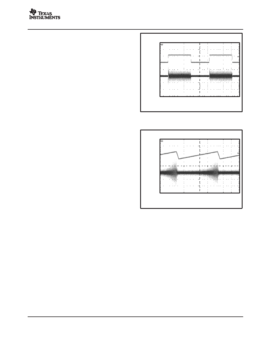
Figure 64 shows the output waveform resulting from a step
change in the control voltage, and Figure 65 shows the
output voltage resulting when the control voltage is a
full-scale ramp.
Time (400ns/div)
Channel 1
V
CNTL
(2V/div)
Channel 2
Output
(20mV/div)
Figure 64. Response to Step Change of VCNTL
Time (400ns/div)
Channel 1
V
CNTL
(2V/div)
Channel 2
Output
(20mV/div)
Figure 65. Response to Ramp Change of VCNTL
The exponential gain control characteristic is achieved
through a piecewise approximation to a perfectly smooth
exponential curve. Eight FETs, operated as variable
resistors whose value is progressively 1/2 of the value of
the adjacent parallel FET, are turned on progressively, or
their value is lowered to create the exponential gain
characteristic. This characteristic can be shown in the
following way. An exponential such as y = ex increases in
the y dimension by a constant ratio as the x dimension
increases by a constant linear amount. In other words, for
a constant (x1 x2), the ratio ex1/ex2 remains the same.
When FETs used as variable resistors are placed in
parallel, the attenuation characteristic that is created
behaves according to this same exponential characteristic
at discrete points as a function of the control voltage.
It
does
not
perfectly
obey
an
ideal
exponential
characteristic at other points; however, an 8-section
approximation yields a
±1dB error to an ideal curve.
(7)
相關(guān)PDF資料 |
PDF描述 |
|---|---|
| VCA2615RGZR | SPECIALTY ANALOG CIRCUIT, PQCC48 |
| VCA3-103-60M00 | CRYSTAL OSCILLATOR, CLOCK, 60 MHz, HCMOS/TTL OUTPUT |
| VCA3-A3F-FREQ | CRYSTAL OSCILLATOR, CLOCK, 0.32768 MHz - 160 MHz, CMOS OUTPUT |
| VCA3-A5D-FREQ | CRYSTAL OSCILLATOR, CLOCK, 0.32768 MHz - 160 MHz, CMOS OUTPUT |
| VCA3-C3H-FREQ | CRYSTAL OSCILLATOR, CLOCK, 0.32768 MHz - 160 MHz, CMOS OUTPUT |
相關(guān)代理商/技術(shù)參數(shù) |
參數(shù)描述 |
|---|---|
| VCA2615PFBT | 功能描述:特殊用途放大器 2Ch Variable Gain Amplifier RoHS:否 制造商:Texas Instruments 通道數(shù)量:Single 共模抑制比(最小值): 輸入補償電壓: 工作電源電壓:3 V to 5.5 V 電源電流:5 mA 最大功率耗散: 最大工作溫度:+ 70 C 最小工作溫度:- 40 C 安裝風格:SMD/SMT 封裝 / 箱體:QFN-20 封裝:Reel |
| VCA2615RGZR | 功能描述:特殊用途放大器 2-Channel Variable Gain Amplifier RoHS:否 制造商:Texas Instruments 通道數(shù)量:Single 共模抑制比(最小值): 輸入補償電壓: 工作電源電壓:3 V to 5.5 V 電源電流:5 mA 最大功率耗散: 最大工作溫度:+ 70 C 最小工作溫度:- 40 C 安裝風格:SMD/SMT 封裝 / 箱體:QFN-20 封裝:Reel |
| VCA2615RGZRG4 | 功能描述:特殊用途放大器 2-Channel Variable Gain Amplifier RoHS:否 制造商:Texas Instruments 通道數(shù)量:Single 共模抑制比(最小值): 輸入補償電壓: 工作電源電壓:3 V to 5.5 V 電源電流:5 mA 最大功率耗散: 最大工作溫度:+ 70 C 最小工作溫度:- 40 C 安裝風格:SMD/SMT 封裝 / 箱體:QFN-20 封裝:Reel |
| VCA2615RGZT | 功能描述:特殊用途放大器 2-Channel Variable Gain Amplifier RoHS:否 制造商:Texas Instruments 通道數(shù)量:Single 共模抑制比(最小值): 輸入補償電壓: 工作電源電壓:3 V to 5.5 V 電源電流:5 mA 最大功率耗散: 最大工作溫度:+ 70 C 最小工作溫度:- 40 C 安裝風格:SMD/SMT 封裝 / 箱體:QFN-20 封裝:Reel |
| VCA2615RGZTG4 | 功能描述:特殊用途放大器 2-Channel Variable Gain Amplifier RoHS:否 制造商:Texas Instruments 通道數(shù)量:Single 共模抑制比(最小值): 輸入補償電壓: 工作電源電壓:3 V to 5.5 V 電源電流:5 mA 最大功率耗散: 最大工作溫度:+ 70 C 最小工作溫度:- 40 C 安裝風格:SMD/SMT 封裝 / 箱體:QFN-20 封裝:Reel |
發(fā)布緊急采購,3分鐘左右您將得到回復。