- 您現(xiàn)在的位置:買賣IC網(wǎng) > PDF目錄359317 > V292BMC (Electronic Theatre Controls, Inc.) HIGH PERFORMANCE BURST DRAM CONTROLLER FOR Am29030/40 PROCESSORS PDF資料下載
參數(shù)資料
| 型號: | V292BMC |
| 廠商: | Electronic Theatre Controls, Inc. |
| 英文描述: | HIGH PERFORMANCE BURST DRAM CONTROLLER FOR Am29030/40 PROCESSORS |
| 中文描述: | 爆高性能的DRAM控制器的Am29030/40處理器 |
| 文件頁數(shù): | 3/14頁 |
| 文件大?。?/td> | 108K |
| 代理商: | V292BMC |
V292BMC Rev.D
Copyright 1998, V3 Semiconductor Corp.
V292BMC Rev D Data Sheet Rev 3.2
3
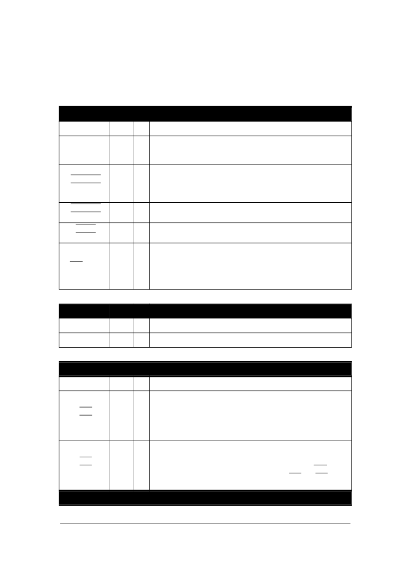
Table 3: Signal Descriptions
Memory Interface Signals
Signal
Type
R
a
Description
AA[11:0]
AB[11:0]
O
12-3
X
Leaf A and B row and column address, multiplexed on the same
pins. When non-interleaved operation is selected, only address bus
AA should be used.
RASA[3:0]
RASB[3:0]
O
12-3
H
Row Address Strobe. These strobes indicate the presence of a valid
row address on busses AA(B)[11:0]. These signals are to be con-
nected one to each 32-bit leaf of memory.
CASA[3:0]
CASB[3:0]
O
12-3
H
Column Address Strobe. These strobes latch a column address from
AA(B)[11:0]. They are assigned one to each byte in a leaf.
MWEA
MWEB
O
12-3
H
Memory Write Enable. These are the DRAM write strobes. One is
supplied for each leaf to minimize signal loading.
RFS/AUXT
O
12
H
Refresh in progress. This output is multi-function signal. The signal
name, as it appears on the logic symbol, is the default signal names.
This signal gives notice that a refresh cycle is to be executed. The
timing leads RAS only refresh by one cycle. The output may also
function as AUX timer interrupt.
Configuration
Signal
Type
R
Description
MOD4
I
Selects Modulo 4 (word) bursting for multiplexed address AA(B).
Buffer Controls Signals
Signal
Type
R
Description
TXA
TXB
O
12
H
Data Transmit A and B. These outputs are multi-function signals.
The signal names, as they appear on the logic symbol, are the
default signal names (Mode 0). The purpose of these outputs is to
control buffer output enables during data read transactions and, in
effect, control the multiplexing of data from each memory leaf onto
the Am29030/40 data bus.
These outputs are mode independent, however, the timing of the
signals change for different operational modes. They control trans-
parent latches that hold data transmitted during a write transaction.
In modes 0 and 1, the latch controls follow the timing of CAS for
each leaf, while in modes 2 and 3 the timing of LEA and LEB is
shortened to 1/2 clock.
LEA
LEB
O
12
L
Local Bus Interface
相關(guān)PDF資料 |
PDF描述 |
|---|---|
| V29C31001B-70P | 1 MEGABIT 131,072 x 8 BIT 5 VOLT CMOS FLASH MEMORY |
| V29C31004B | 4 MEGABIT 524,288 x 8 BIT 3.3 VOLT CMOS FLASH MEMORY |
| V29C51000B | 512K Bit 5 Volt CMOS Flash Memory(512K位5V CMOS閃速存儲器) |
| V29C51000T-90P | 512K BIT 65,536 x 8 BIT 5 VOLT CMOS FLASH MEMORY |
| V29C51001B | 1 MEGA Bit 5 Volt CMOS Flash Memory(1M位5V CMOS閃速存儲器) |
相關(guān)代理商/技術(shù)參數(shù) |
參數(shù)描述 |
|---|---|
| V292BMC-25LP | 制造商:未知廠家 制造商全稱:未知廠家 功能描述:DRAM Controller |
| V292BMC-33LP | 制造商:未知廠家 制造商全稱:未知廠家 功能描述:HIGH PERFORMANCE BURST DRAM CONTROLLER FOR Am29030/40 PROCESSORS |
| V292BMC-40LP | 制造商:Rochester Electronics LLC 功能描述: 制造商:QuickLogic Corporation 功能描述: |
| V292PBC-33 | 制造商:未知廠家 制造商全稱:未知廠家 功能描述:PCI Bus Interface/Controller |
| V292PBC-33LP | 制造商:未知廠家 制造商全稱:未知廠家 功能描述:PCI Bus Interface/Controller |
發(fā)布緊急采購,3分鐘左右您將得到回復(fù)。