- 您現(xiàn)在的位置:買賣IC網(wǎng) > PDF目錄297644 > UPD789304GK-XXX-9ET 8-BIT, MROM, 5 MHz, MICROCONTROLLER, PQFP64 PDF資料下載
參數(shù)資料
| 型號(hào): | UPD789304GK-XXX-9ET |
| 元件分類: | 微控制器/微處理器 |
| 英文描述: | 8-BIT, MROM, 5 MHz, MICROCONTROLLER, PQFP64 |
| 封裝: | 12 X 12 MM, PLASTIC, TQFP-64 |
| 文件頁數(shù): | 227/328頁 |
| 文件大小: | 3881K |
| 代理商: | UPD789304GK-XXX-9ET |
第1頁第2頁第3頁第4頁第5頁第6頁第7頁第8頁第9頁第10頁第11頁第12頁第13頁第14頁第15頁第16頁第17頁第18頁第19頁第20頁第21頁第22頁第23頁第24頁第25頁第26頁第27頁第28頁第29頁第30頁第31頁第32頁第33頁第34頁第35頁第36頁第37頁第38頁第39頁第40頁第41頁第42頁第43頁第44頁第45頁第46頁第47頁第48頁第49頁第50頁第51頁第52頁第53頁第54頁第55頁第56頁第57頁第58頁第59頁第60頁第61頁第62頁第63頁第64頁第65頁第66頁第67頁第68頁第69頁第70頁第71頁第72頁第73頁第74頁第75頁第76頁第77頁第78頁第79頁第80頁第81頁第82頁第83頁第84頁第85頁第86頁第87頁第88頁第89頁第90頁第91頁第92頁第93頁第94頁第95頁第96頁第97頁第98頁第99頁第100頁第101頁第102頁第103頁第104頁第105頁第106頁第107頁第108頁第109頁第110頁第111頁第112頁第113頁第114頁第115頁第116頁第117頁第118頁第119頁第120頁第121頁第122頁第123頁第124頁第125頁第126頁第127頁第128頁第129頁第130頁第131頁第132頁第133頁第134頁第135頁第136頁第137頁第138頁第139頁第140頁第141頁第142頁第143頁第144頁第145頁第146頁第147頁第148頁第149頁第150頁第151頁第152頁第153頁第154頁第155頁第156頁第157頁第158頁第159頁第160頁第161頁第162頁第163頁第164頁第165頁第166頁第167頁第168頁第169頁第170頁第171頁第172頁第173頁第174頁第175頁第176頁第177頁第178頁第179頁第180頁第181頁第182頁第183頁第184頁第185頁第186頁第187頁第188頁第189頁第190頁第191頁第192頁第193頁第194頁第195頁第196頁第197頁第198頁第199頁第200頁第201頁第202頁第203頁第204頁第205頁第206頁第207頁第208頁第209頁第210頁第211頁第212頁第213頁第214頁第215頁第216頁第217頁第218頁第219頁第220頁第221頁第222頁第223頁第224頁第225頁第226頁當(dāng)前第227頁第228頁第229頁第230頁第231頁第232頁第233頁第234頁第235頁第236頁第237頁第238頁第239頁第240頁第241頁第242頁第243頁第244頁第245頁第246頁第247頁第248頁第249頁第250頁第251頁第252頁第253頁第254頁第255頁第256頁第257頁第258頁第259頁第260頁第261頁第262頁第263頁第264頁第265頁第266頁第267頁第268頁第269頁第270頁第271頁第272頁第273頁第274頁第275頁第276頁第277頁第278頁第279頁第280頁第281頁第282頁第283頁第284頁第285頁第286頁第287頁第288頁第289頁第290頁第291頁第292頁第293頁第294頁第295頁第296頁第297頁第298頁第299頁第300頁第301頁第302頁第303頁第304頁第305頁第306頁第307頁第308頁第309頁第310頁第311頁第312頁第313頁第314頁第315頁第316頁第317頁第318頁第319頁第320頁第321頁第322頁第323頁第324頁第325頁第326頁第327頁第328頁
CHAPTER 22
ELECTRICAL SPECIFICATIONS
User’s Manual U14800EJ3V0UD
302
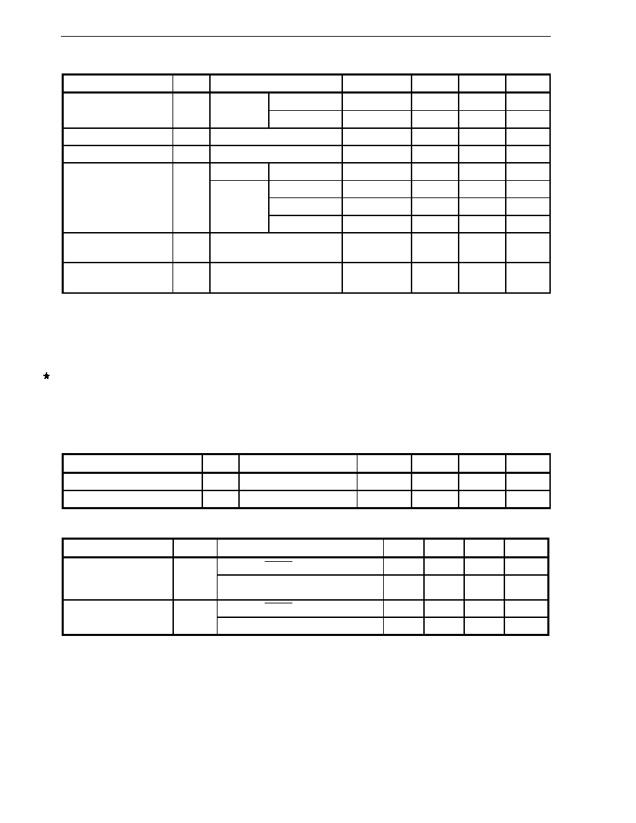
LCD Characteristics (TA = –40 to +85
°C, VDD = 1.8 to 5.5 V)
Parameter
Symbol
Conditions
MIN.
TYP.
MAX.
Unit
GAIN = 1
0.84
1.0
1.165
V
LCD output voltage
variation range
VLCD2
C1 to C4
Note 1
= 0.47
F
GAIN = 0
1.26
1.5
1.74
V
Doubler output
VLCD1
C1 to C4
Note 1 = 0.47
F
2 VLCD2– 0.1
2.0 VLCD2
V
Tripler output
VLCD0
C1 to C4
Note 1 = 0.47
F
3 VLCD2– 0.15
3.0 VLCD2
V
GAIN = 0
1.8
≤ VDD ≤ 5.5 V
0.5
s
5.0
≤ VDD ≤ 5.5 V
2.0
s
4.5
≤ VDD < 5.0 V
1.0
s
Voltage boost wait time
Note 2
tVAWAIT
GAIN = 1
1.8
≤ VDD < 4.5 V
0.5
s
LCD output voltage
differential
Note 3 (common)
VODC
IO =
±5
A
0
±0.2
V
LCD output voltage
differential
Note 3 (segment)
VODS
IO =
±1
A
0
±0.2
V
Notes 1. This is a capacitor that is connected between voltage pins used to drive the LCD.
C1: Capacitor connected between CAPH and CAPL
C2: Capacitor connected between VLC0 and VSS
C3: Capacitor connected between VLC1 and VSS
C4: Capacitor connected between VLC2 and VSS
2. This is the wait time from when voltage boost is started (VAON0 = 1) until display is enabled (LCDON0
= 1).
3. The voltage differential is the difference between the segment and common signal output’s actual and
ideal output voltages.
Data Memory STOP Mode Low Supply Voltage Data Retention Characteristics (TA = –40 to +85
°C)
Parameter
Symbol
Conditions
MIN.
TYP.
MAX.
Unit
Data retention power supply voltage VDDDR
1.8
5.5
V
Release signal set time
tSREL
0
s
Oscillation Stabilization Wait Time (TA = –40 to +85
°C, VDD = 1.8 to 5.5 V)
Parameter
Symbol
Conditions
MIN.
TYP.
MAX.
Unit
Release by RESET
2
15
/fX
s
Oscillation stabilization wait
time
Note 1 (ceramic/crystal
oscillation)
tWAIT
Release by interrupt
Note 2
s
Release by RESET
2
7
/fCC
s
Oscillation stabilization wait
time (RC oscillation)
tWAIT
Release by interrupt
2
7
/fCC
s
Notes 1. Use a resonator whose oscillation stabilizes within the oscillation stabilization wait time.
2. Selection of 2
12/fX, 215/fX, or 217/fX is possible with bits 0 to 2 (OSTS0 to OSTS2) of the oscillation
stabilization time select register (OSTS).
Remarks 1. fX:
Main system clock oscillation frequency (ceramic/crystal oscillation)
2. fCC:
Main system clock oscillation frequency (RC oscillation)
相關(guān)PDF資料 |
PDF描述 |
|---|---|
| UPSD3253B-40T6 | 8-BIT, FLASH, 40 MHz, MICROCONTROLLER, PQFP52 |
| UPSD3334D-40U6 | 8-BIT, FLASH, 40 MHz, MICROCONTROLLER, PQFP80 |
| US1001FL | 0.5 A, 100 V, SILICON, SIGNAL DIODE |
| US1A-HE3 | 1 A, 50 V, SILICON, SIGNAL DIODE, DO-214AC |
| US1B-HE3 | 1 A, 100 V, SILICON, SIGNAL DIODE, DO-214AC |
相關(guān)代理商/技術(shù)參數(shù) |
參數(shù)描述 |
|---|---|
| UPD789407AGC-029-8BT | 制造商:Renesas Electronics Corporation 功能描述: |
| UPD789416AGC-017-8BTA | 制造商:Renesas Electronics Corporation 功能描述: |
| UPD789417AGK-A06-9EU | 制造商:Renesas Electronics Corporation 功能描述: |
| UPD789445GB-8EU-A | 制造商:Renesas Electronics Corporation 功能描述: |
| UPD789488GK-517-9EU | 制造商:NEC Electronics Corporation 功能描述: |
發(fā)布緊急采購,3分鐘左右您將得到回復(fù)。