- 您現(xiàn)在的位置:買賣IC網(wǎng) > PDF目錄384046 > UPD784915A (NEC Corp.) 16-BIT SINGLE-CHIP MICROCONTROLLERS PDF資料下載
參數(shù)資料
| 型號: | UPD784915A |
| 廠商: | NEC Corp. |
| 英文描述: | 16-BIT SINGLE-CHIP MICROCONTROLLERS |
| 中文描述: | 16位單晶片微控制器 |
| 文件頁數(shù): | 68/86頁 |
| 文件大小: | 446K |
| 代理商: | UPD784915A |
第1頁第2頁第3頁第4頁第5頁第6頁第7頁第8頁第9頁第10頁第11頁第12頁第13頁第14頁第15頁第16頁第17頁第18頁第19頁第20頁第21頁第22頁第23頁第24頁第25頁第26頁第27頁第28頁第29頁第30頁第31頁第32頁第33頁第34頁第35頁第36頁第37頁第38頁第39頁第40頁第41頁第42頁第43頁第44頁第45頁第46頁第47頁第48頁第49頁第50頁第51頁第52頁第53頁第54頁第55頁第56頁第57頁第58頁第59頁第60頁第61頁第62頁第63頁第64頁第65頁第66頁第67頁當(dāng)前第68頁第69頁第70頁第71頁第72頁第73頁第74頁第75頁第76頁第77頁第78頁第79頁第80頁第81頁第82頁第83頁第84頁第85頁第86頁
μ
PD784915A, 784916A
68
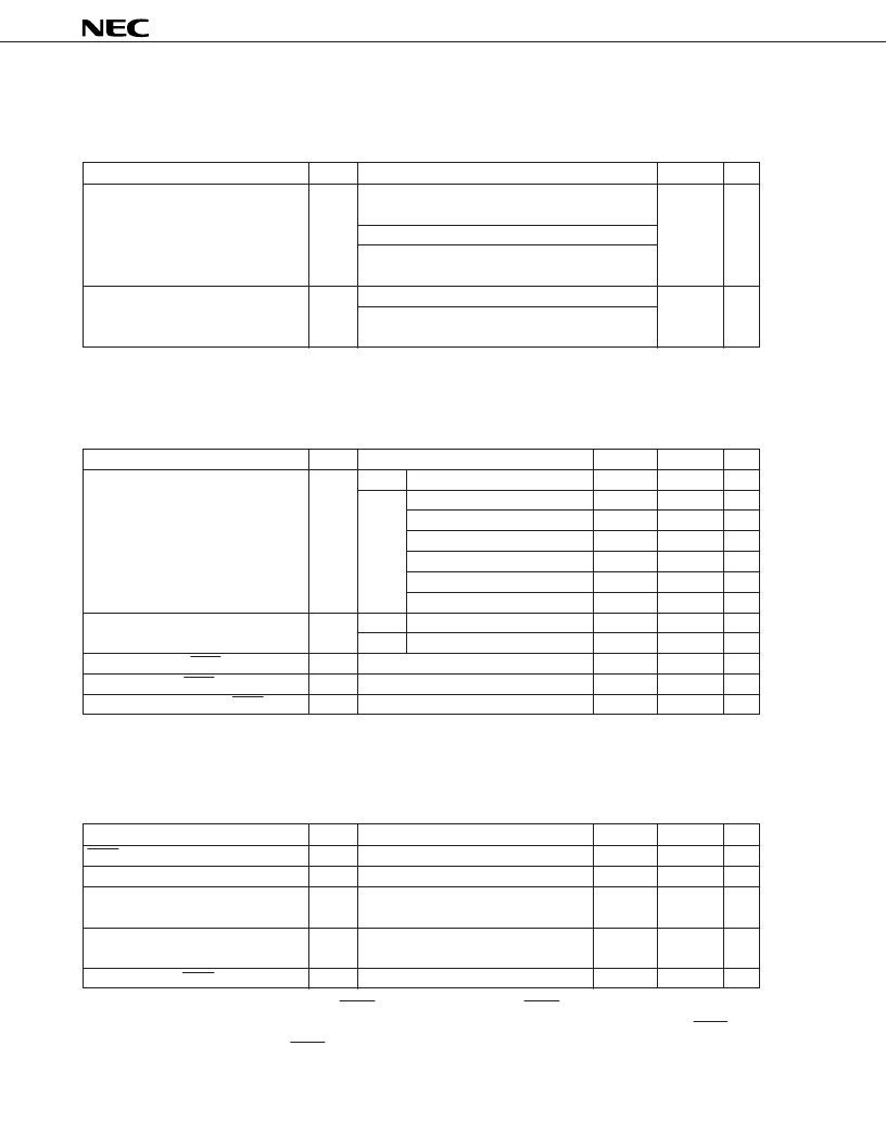
AC Characteristics
CPU and peripheral circuit operation clock (T
A
= –10 to +70
°
C, V
DD
= AV
DD
= 4.5 to 5.5 V, V
SS
= AV
SS
= 0 V)
Parameter
Symbol
Condition
TYP.
Unit
CPU operation clock cycle time
t
CLK
f
XX
= 16 MHz
V
DD
= AV
DD
= 4.0 to 5.5 V
125
ns
CPU Function only
f
XX
= 16 MHz
f
XX
= 8 MHz
low-frequency oscillation mode
(Bit 7 of CC = 1)
Peripheral operation clock cycle time
t
CLK1
f
XX
= 16 MHz
125
ns
f
XX
= 8MHz
low-frequency oscillation mode
(Bit 7 of CC = 1)
Serial interface
(1) SIOn: n = 1 or 2 (T
A
= –10 to +70
°
C, V
DD
= AV
DD
= 4.5 to 5.5 V, V
SS
= AV
SS
= 0 V)
Parameter
Symbol
Condition
MIN.
MAX.
Unit
Serial clock cycle time
t
CYSK
Input
External clock
1.0
μ
s
μ
s
μ
s
μ
s
μ
s
μ
s
μ
s
Output
f
CLK1
/8
1.0
f
CLK1
/16
2.0
f
CLK1
/32
4.0
f
CLK1
/64
8.0
f
CLK1
/128
16
f
CLK1
/256
32
Serial clock high- and low-level widths
t
WSKH
Input
External clock
420
ns
t
WSKL
Output
Internal clock
t
CYSK
/2 – 50
ns
SIn setup time (vs. SCKn
↑
)
SIn hold time (vs. SCKn
↑
)
SOn output delay time (vs. SCKn
↓
)
t
SSSK
100
ns
t
HSSK
400
ns
t
DSSK
0
300
ns
Remarks 1.
f
CLK1
: operating clock of peripheral circuit (8 MHz)
2.
n = 1 or 2
(2) SIO2 only (T
A
= –10 to +70
°
C, V
DD
= AV
DD
= 4.5 to 5.5 V, V
SS
= AV
SS
= 0 V)
Parameter
Symbol
Condition
MIN.
MAX.
Unit
SCK2(8)
↑→
STBR
↑
t
DSTRB
t
WSKH
t
CYSK
Strobe high-level width
t
WSTRB
t
CYSK
– 30
t
CYSK
+ 30
ns
BUSY setup time
t
SBUSY
100
ns
(vs. BUSY detection timing)
BUSY hold time
t
HBUSY
100
ns
(vs. BUSY detection timing)
BUSY inactive
→
SCK2(1)
↓
t
LBUSY
t
CYSK
+ t
WSKH
Remarks 1.
The value in ( ) following SCK2 indicates the number of SCK2.
2.
BUSY is detected after the time (n+2) x t
CYSK
(n = 0, 1, and so on) has elapsed relative to SCK2 (8)
↑
.
3.
BUSY inactive
→
SCK2 (1)
↓
is the value when data write to SIO2 has been completed.
相關(guān)PDF資料 |
PDF描述 |
|---|---|
| UPD784915AGF | 16-BIT SINGLE-CHIP MICROCONTROLLERS |
| UPD784916A | 16-BIT SINGLE-CHIP MICROCONTROLLERS |
| UPD784916AGF | 16-BIT SINGLE-CHIP MICROCONTROLLERS |
| UPD784915B | 16-BIT SINGLE-CHIP MICROCONTROLLERS |
| UPD784915BGF | 16-BIT SINGLE-CHIP MICROCONTROLLERS |
相關(guān)代理商/技術(shù)參數(shù) |
參數(shù)描述 |
|---|---|
| UPD784935AGF-113-3BA | 制造商:NEC Electronics Corporation 功能描述: |
| UPD784938AGF-188-3BA | 制造商:NEC Electronics Corporation 功能描述: |
| UPD789104AMC(A)-968-5A4-E2 | 制造商:Renesas Electronics Corporation 功能描述: |
| UPD789104AMC-671-5A4-E1 | 制造商:Renesas Electronics Corporation 功能描述: |
| UPD789104AMC-672-5A4-E1 | 制造商:Renesas Electronics Corporation 功能描述: |
發(fā)布緊急采購,3分鐘左右您將得到回復(fù)。