- 您現(xiàn)在的位置:買(mǎi)賣(mài)IC網(wǎng) > PDF目錄384046 > UPD784031 (NEC Corp.) 16/8-BIT SINGLE-CHIP MICROCONTROLLER PDF資料下載
參數(shù)資料
| 型號(hào): | UPD784031 |
| 廠(chǎng)商: | NEC Corp. |
| 英文描述: | 16/8-BIT SINGLE-CHIP MICROCONTROLLER |
| 中文描述: | 16/8-BIT單片機(jī) |
| 文件頁(yè)數(shù): | 13/90頁(yè) |
| 文件大小: | 377K |
| 代理商: | UPD784031 |
第1頁(yè)第2頁(yè)第3頁(yè)第4頁(yè)第5頁(yè)第6頁(yè)第7頁(yè)第8頁(yè)第9頁(yè)第10頁(yè)第11頁(yè)第12頁(yè)當(dāng)前第13頁(yè)第14頁(yè)第15頁(yè)第16頁(yè)第17頁(yè)第18頁(yè)第19頁(yè)第20頁(yè)第21頁(yè)第22頁(yè)第23頁(yè)第24頁(yè)第25頁(yè)第26頁(yè)第27頁(yè)第28頁(yè)第29頁(yè)第30頁(yè)第31頁(yè)第32頁(yè)第33頁(yè)第34頁(yè)第35頁(yè)第36頁(yè)第37頁(yè)第38頁(yè)第39頁(yè)第40頁(yè)第41頁(yè)第42頁(yè)第43頁(yè)第44頁(yè)第45頁(yè)第46頁(yè)第47頁(yè)第48頁(yè)第49頁(yè)第50頁(yè)第51頁(yè)第52頁(yè)第53頁(yè)第54頁(yè)第55頁(yè)第56頁(yè)第57頁(yè)第58頁(yè)第59頁(yè)第60頁(yè)第61頁(yè)第62頁(yè)第63頁(yè)第64頁(yè)第65頁(yè)第66頁(yè)第67頁(yè)第68頁(yè)第69頁(yè)第70頁(yè)第71頁(yè)第72頁(yè)第73頁(yè)第74頁(yè)第75頁(yè)第76頁(yè)第77頁(yè)第78頁(yè)第79頁(yè)第80頁(yè)第81頁(yè)第82頁(yè)第83頁(yè)第84頁(yè)第85頁(yè)第86頁(yè)第87頁(yè)第88頁(yè)第89頁(yè)第90頁(yè)
μ
PD784031
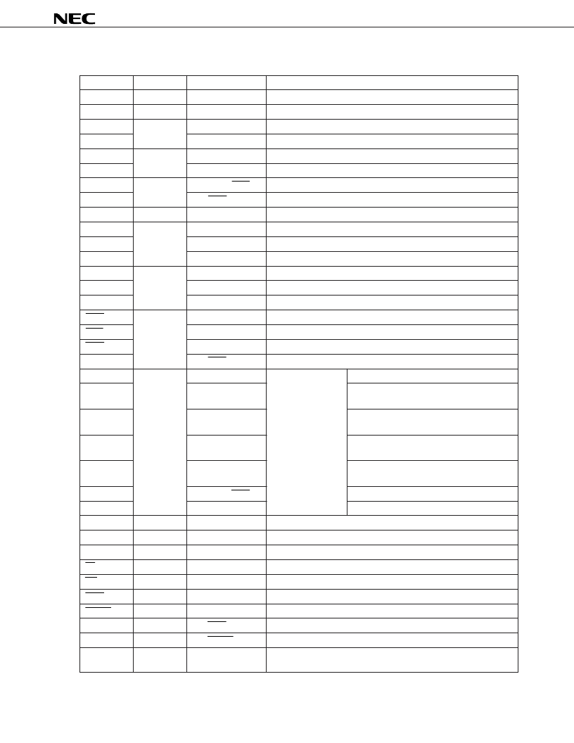
13
Pin
I/O
Dual-function
Function
TO0-TO3
Output
P34-P37
Timer output
CI
Input
P23/INTP2
Input of a count clock for timer/counter 2
R
X
D
Input
P30/SI1
Serial data input (UART0)
R
X
D2
P13/SI2
Serial data input (UART2)
T
X
D
Output
P31/SO1
Serial data output (UART0)
T
X
D2
P14/SO2
Serial data output (UART2)
ASCK
Input
P25/INTP4/SCK1
Baud rate clock input (UART0)
ASCK2
P12/SCK2
Baud rate clock input (UART2)
SDA
I/O
P33/SO0
Serial data I/O (2-wire serial I/O)
SI0
Input
P27
Serial data input (3-wire serial I/O0)
SI1
P30/R
X
D
Serial data input (3-wire serial I/O1)
SI2
P13/R
X
D2
Serial data input (3-wire serial I/O2)
SO0
Output
P33/SDA
Serial data output (3-wire serial I/O0)
SO1
P31/T
X
D
Serial data output (3-wire serial I/O1)
SO2
P14/T
X
D2
Serial data output (3-wire serial I/O2)
SCK0
I/O
P32/SCL
Serial clock I/O (3-wire serial I/O0)
SCK1
P25/INTP4/ASCK
Serial clock I/O (3-wire serial I/O1)
SCK2
P12/ASCK2
Serial clock I/O (3-wire serial I/O2)
SCL
P32/SCK0
Serial clock I/O (2-wire serial I/O)
NMI
Input
P20
External interrupt request
-
INTP0
P21
Input of a count clock for timer/counter 1
Capture/trigger signal for CR11 or CR12
INTP1
P22
Input of a count clock for timer/counter 2
Capture/trigger signal for CR22
INTP2
P23/CI
Input of a count clock for timer/counter 2
Capture/trigger signal for CR21
INTP3
P24
Input of a count clock for timer/counter 0
Capture/trigger signal for CR02
INTP4
P25/ASCK/SCK1
-
INTP5
P26
Input of a conversion start trigger for A/D converter
AD0-AD7
I/O
-
Time multiplexing address/data bus (for connecting external memory)
A8-A15
Output
-
High-order address bus (for connecting external memory)
A16-A19
Output
P60-P63
High-order address bus during address expansion (for connecting external memory)
RD
Output
-
Strobe signal output for reading the contents of external memory
WR
Output
-
Strobe signal output for writing on external memory
WAIT
Input
P66/HLDRQ
Wait signal insertion
REFRQ
Output
P67/HLDAK
Refresh pulse output to external pseudo static memory
HLDRQ
Input
P66/WAIT
Input of bus hold request
HLDAK
Output
P67/REFRQ
Output of bus hold response
ASTB
Output
-
Latch timing output of time multiplexing address (A0-A7) (for
connecting external memory)
6.2 Non-Port Pins (1/2)
相關(guān)PDF資料 |
PDF描述 |
|---|---|
| UPD784031A | 16/8-BIT SINGLE-CHIP MICROCONTROLLER |
| UPD784907 | 16-BIT SINGLE-CHIP MICROCONTROLLER |
| UPD784907GF | 16-BIT SINGLE-CHIP MICROCONTROLLER |
| UPD784908 | 16-BIT SINGLE-CHIP MICROCONTROLLER |
| UPD784908GF | 16-BIT SINGLE-CHIP MICROCONTROLLER |
相關(guān)代理商/技術(shù)參數(shù) |
參數(shù)描述 |
|---|---|
| UPD784031GC-8BT-A | 制造商:Renesas Electronics Corporation 功能描述:MCU 8BIT/16BIT 78K4 CISC ROMLESS 3.3V/5V 80PQFP - Trays 制造商:Renesas Electronics 功能描述:16 制造商:Renesas Electronics 功能描述:16 Cut Tape |
| UPD784031GK-9EU-A | 制造商:Renesas Electronics Corporation 功能描述:16BIT K4 ROMLESS - Bulk |
| UPD784031YGC-8BT | 制造商:Renesas Electronics Corporation 功能描述: |
| UPD784031YGC-8BT-A | 制造商:Renesas Electronics Corporation 功能描述: |
| UPD784031YGK-9EU | 制造商:Renesas Electronics Corporation 功能描述: |
發(fā)布緊急采購(gòu),3分鐘左右您將得到回復(fù)。