- 您現(xiàn)在的位置:買賣IC網(wǎng) > PDF目錄383983 > UPD75212ACW (NEC Corp.) 4-BIT SINGLE-CHIP MICROCOMPUTER PDF資料下載
參數(shù)資料
| 型號(hào): | UPD75212ACW |
| 廠商: | NEC Corp. |
| 英文描述: | 4-BIT SINGLE-CHIP MICROCOMPUTER |
| 中文描述: | 4位單片機(jī) |
| 文件頁(yè)數(shù): | 48/70頁(yè) |
| 文件大小: | 516K |
| 代理商: | UPD75212ACW |
第1頁(yè)第2頁(yè)第3頁(yè)第4頁(yè)第5頁(yè)第6頁(yè)第7頁(yè)第8頁(yè)第9頁(yè)第10頁(yè)第11頁(yè)第12頁(yè)第13頁(yè)第14頁(yè)第15頁(yè)第16頁(yè)第17頁(yè)第18頁(yè)第19頁(yè)第20頁(yè)第21頁(yè)第22頁(yè)第23頁(yè)第24頁(yè)第25頁(yè)第26頁(yè)第27頁(yè)第28頁(yè)第29頁(yè)第30頁(yè)第31頁(yè)第32頁(yè)第33頁(yè)第34頁(yè)第35頁(yè)第36頁(yè)第37頁(yè)第38頁(yè)第39頁(yè)第40頁(yè)第41頁(yè)第42頁(yè)第43頁(yè)第44頁(yè)第45頁(yè)第46頁(yè)第47頁(yè)當(dāng)前第48頁(yè)第49頁(yè)第50頁(yè)第51頁(yè)第52頁(yè)第53頁(yè)第54頁(yè)第55頁(yè)第56頁(yè)第57頁(yè)第58頁(yè)第59頁(yè)第60頁(yè)第61頁(yè)第62頁(yè)第63頁(yè)第64頁(yè)第65頁(yè)第66頁(yè)第67頁(yè)第68頁(yè)第69頁(yè)第70頁(yè)
48
μ
PD75212A
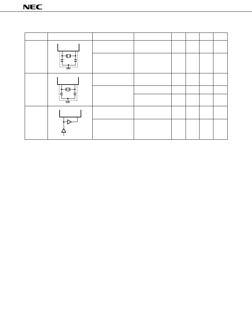
X1
X2
C1
C2
X1
X2
C1
C2
MAIN SYSTEM CLOCK OSCILLATOR CHARACTERISTICS (Ta = –40 to +85
°
C, V
DD
= 2.7 to 6.0 V )
V
DD
= Oscillation
voltage range
After V
DD
reaches the
minimum value in
the oscillation
voltage range
V
DD
= 4.5 to 6.0 V
Oscillator frequency
(f
XX
)
*2
Oscillation
stabilization time
*3
Oscillator frequency
(f
XX
)
*2
Oscillation stabilization
time
*3
X1 input frequency
(f
X
)
*2
X1 input high and low
level widths (t
XH
, t
XL
)
X1
X2
μ
PD74HCU04
2.0
2.0
2.0
100
4.19
5.0
*4
4
5.0
*4
10
30
5.0
*4
250
MHz
ms
MHz
ms
ms
MHz
ns
MIN.
TYP.
MAX.
UNIT
TEST CONDITIONS
PARAMETER
RECOMMENDED CIRCUIT
RESONATOR
Ceramic
resonator
*1
Crystal
resonator
*1
External
clock
*
1.
Refer to
RECOMMENDED OSCILLATOR CONSTANTS
.
2.
Oscillator characteristics only. Refer to the description of AC characteristics for details of instruction execution
time.
3.
Time required for oscillation to become stabilized after V
DD
reaches the minimum value in the oscillation
voltage range or STOP mode release.
4.
When oscillator frequency is “4.19 < f
XX
< 5.0 MHz”, do not select “PCC = 0011” as instruction execution time.
If “PCC = 0011” is selected, 1 machine cycle becomes less than 0.95
μ
s, with the result that the specified MIN.
value of 0.95
μ
s cannot be observed.
Note
When the main system clock oscillator is used, the following should be noted concerning wiring in the area
in the figure enclosed by a dotted line to prevent the influence of wiring capacitance, etc.
The wiring should be kept as short as possible.
No other signal lines should be crossed. Keep away from lines carrying a high fluctuating current.
The oscillator capacitor grounding point should always be at the same potential as V
SS
. Do not connect
to a ground pattern carrying a high current.
A signal should not be taken from the oscillator.
#
相關(guān)PDF資料 |
PDF描述 |
|---|---|
| UPD75212AGF | 4-BIT SINGLE-CHIP MICROCOMPUTER |
| UPD75216 | 4-BIT SINGLE-CHIP MICROCOMPUTER |
| UPD75216A | 4-BIT SINGLE-CHIP MICROCOMPUTER |
| UPD75216ACW | 4-BIT SINGLE-CHIP MICROCOMPUTER |
| UPD75216AGF | 4-BIT SINGLE-CHIP MICROCOMPUTER |
相關(guān)代理商/技術(shù)參數(shù) |
參數(shù)描述 |
|---|---|
| UPD753012AGC-P33-8BT-A | 制造商:Renesas Electronics Corporation 功能描述: |
| UPD753016AGC-P29-8BT | 制造商:Renesas Electronics Corporation 功能描述: |
| UPD75304GF-407-3B9 | 制造商:Renesas Electronics Corporation 功能描述: |
| UPD75306G182 | 制造商:Panasonic Industrial Company 功能描述:IC |
| UPD75308F478 | 制造商:Panasonic Industrial Company 功能描述:IC |
發(fā)布緊急采購(gòu),3分鐘左右您將得到回復(fù)。