- 您現(xiàn)在的位置:買賣IC網(wǎng) > PDF目錄383983 > UPD75008CU (NEC Corp.) 4-BIT SINGLE-CHIP MICROCOMPUTER PDF資料下載
參數(shù)資料
| 型號: | UPD75008CU |
| 廠商: | NEC Corp. |
| 英文描述: | 4-BIT SINGLE-CHIP MICROCOMPUTER |
| 中文描述: | 4位單片機 |
| 文件頁數(shù): | 41/66頁 |
| 文件大小: | 542K |
| 代理商: | UPD75008CU |
第1頁第2頁第3頁第4頁第5頁第6頁第7頁第8頁第9頁第10頁第11頁第12頁第13頁第14頁第15頁第16頁第17頁第18頁第19頁第20頁第21頁第22頁第23頁第24頁第25頁第26頁第27頁第28頁第29頁第30頁第31頁第32頁第33頁第34頁第35頁第36頁第37頁第38頁第39頁第40頁當前第41頁第42頁第43頁第44頁第45頁第46頁第47頁第48頁第49頁第50頁第51頁第52頁第53頁第54頁第55頁第56頁第57頁第58頁第59頁第60頁第61頁第62頁第63頁第64頁第65頁第66頁
μ
PD75004, 75006, 75008
41
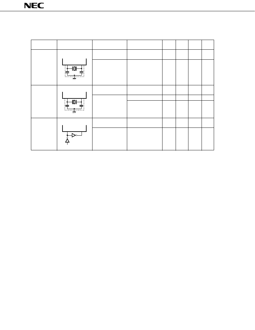
MAIN SYSTEM CLOCK OSCILLATOR CIRCUIT CHARACTERISTICS
(T
a
= -40 to +85
°
C, V
DD
= 2.7 to 6.0 V)
Oscillator
Recommended
Constants
Item
Conditions
MIN.
TYP.
MAX.
Unit
Ceramic
Oscillation
frequency(f
XX
)*
1
V
DD
= Oscillation
voltage range
1.0
5.0
MHz
Oscillation stabiliza- After V
DD
come to
tion time*
2
MIN. of oscillation
voltage range
4
ms
Crystal
Oscillation
frequency (f
XX
)*
1
Oscillation stabiliza- V
DD
= 4.5 to 6.0 V
tion time*
2
1.0
4.19
5.0
MHz
10
ms
30
ms
External Clock
X1 input frequency
(f
X
)*
1
X1 input high-,
low-level widths
(t
XH
, t
XL
)
1.0
5.0
MHz
100
500
ns
*1: The oscillation frequency and X1 input frequency are indicated only to express the characteristics
of the oscillator circuit. For instruction execution time, refer to AC Characteristics.
2: Time required for oscillation to stabilize after V
DD
has been applied or the STOP mode has been
released.
3: When the oscillation frequency is 4.19 MHz
<
fx
≤
5.0 MHz, do not select PCC = 0011 as the
instruction execution time: otherwise, one machine cycle is set to less than 0.95
μ
s, falling short
of the rated minimum value of 0.95
μ
s.
Note:
When using the oscillation circuit of the main system clock, wire the portion enclosed in dotted
line in the figures as follows to avoid adverse influences on the wiring capacity:
Keep the wiring length as short as possible.
Do not cross the wiring over the other signal lines.
Do not route the wiring in the vicinity of lines through which a high alternating current flows.
Always keep the ground point of the capacitor of the osccillator circuit at the same potential
as V
SS
. Do not connect the ground pattern through which a high current flows.
Do not extract signals from the oscillation circuit.
X1
X2
C1
C2
X1
X2
C1
C2
X1
X2
PD74HCU04
μ
*
3
*
3
*
3
#
#
相關PDF資料 |
PDF描述 |
|---|---|
| UPD75008GB | 4-BIT SINGLE-CHIP MICROCOMPUTER |
| UPD7514 | 4-BIT, SINGLE-CHIP CMOS MICROCOMPUTER WITH LCD CONTROLLER/DRIVER |
| UPD7514G-12 | 4-BIT, SINGLE-CHIP CMOS MICROCOMPUTER WITH LCD CONTROLLER/DRIVER |
| UPD75212A | 4-BIT SINGLE-CHIP MICROCOMPUTER |
| UPD75212ACW | 4-BIT SINGLE-CHIP MICROCOMPUTER |
相關代理商/技術參數(shù) |
參數(shù)描述 |
|---|---|
| UPD7507C189 | 制造商:Panasonic Industrial Company 功能描述:IC |
| UPD7508CU265 | 制造商:Panasonic Industrial Company 功能描述:IC |
| UPD75208 | 制造商:Panasonic Industrial Company 功能描述:IC |
| UPD753012AGC-P33-8BT-A | 制造商:Renesas Electronics Corporation 功能描述: |
| UPD753016AGC-P29-8BT | 制造商:Renesas Electronics Corporation 功能描述: |
發(fā)布緊急采購,3分鐘左右您將得到回復。