- 您現(xiàn)在的位置:買賣IC網(wǎng) > PDF目錄383979 > UPD16700 (NEC Corp.) 256-OUTPUT TFT-LCD GATE DRIVER PDF資料下載
參數(shù)資料
| 型號: | UPD16700 |
| 廠商: | NEC Corp. |
| 英文描述: | 256-OUTPUT TFT-LCD GATE DRIVER |
| 中文描述: | 256輸出的TFT - LCD柵極驅(qū)動器 |
| 文件頁數(shù): | 4/12頁 |
| 文件大?。?/td> | 76K |
| 代理商: | UPD16700 |
Data Sheet S14085EJ1V1DS00
4
μ
PD16700
3. PIN FUNCTIONS
Pin Symbol
Pin Name
Description
O
1
to O
256
Driver output
These pins output scan signals that drive the vertical direction (gate lines) of a TFT-LCD.
The output signals change in synchronization with the rising edge of shift clock CLK. The
driver output amplitude is V
DD2
- V
EE2
.
R,/L = H (right shift) : STVR
→
O
1
→
O
256
→
STVL
R,/L = L (left shift) : STVL
→
O
256
→
O
1
→
STVR
This is the input of the internal shift register. The start pulse is read at the rising edge of shift
clock CLK, and scan signals are output from the driver output pins. The input level is a
CMOS (3.3 V) level. The start pulse is output at the falling edge of the 256th clock of shigt
clock CLK, and is cleared at the falling edge of the 257th clock. The output level is V
DD1
-
V
SS
(logic level).
This pin inputs a shift clock to the internal shift register.
The shift operation is performed in synchronization with the rising edge of this input.
When this pin goes H, the driver output is fixed to V
EE2
level.
The shift register is not cleared.
OE
1
: O
1
, O
4
, ... O
250
, O
253
, O
256
OE
1
: O
2
, O
5
, ... O
251
, O
254
OE
1
: O
3
, O
6
, ... O
252
, O
255
When this pin goes L, the driver output is fixed to V
DD2
level. The shift register is not cleared.
This pin has priority over OE
1
to OE
3
.
3.3 V
±
0.3 V
15 to 25 V
The driver output : H level
Connect this pin to the ground of the system.
R,/L
Shift direction select
input
Start pulse
input/output
STVR,
STVL
CLK
Shift clock input
OE
1
,OE
2
,OE
3
Output enable input
AO
All-on control
V
DD1
Logic power supply
V
DD2
Driver positive power
supply
Logic ground
V
SS
V
EE1
Negative Power
supply for internal
operation
Driver negative
power supply
–15 to –5 V
V
EE2
The driver output : L level (V
EE2
-V
EE1
< 6.0 V)
Cautions 1.
To prevent latch up, turn on power to V
DD1
, V
EE1/2
, V
DD2
, and logic input in this order. Turn off
power in the reverse order. These power up/down sequence must be observed also during
transition period.
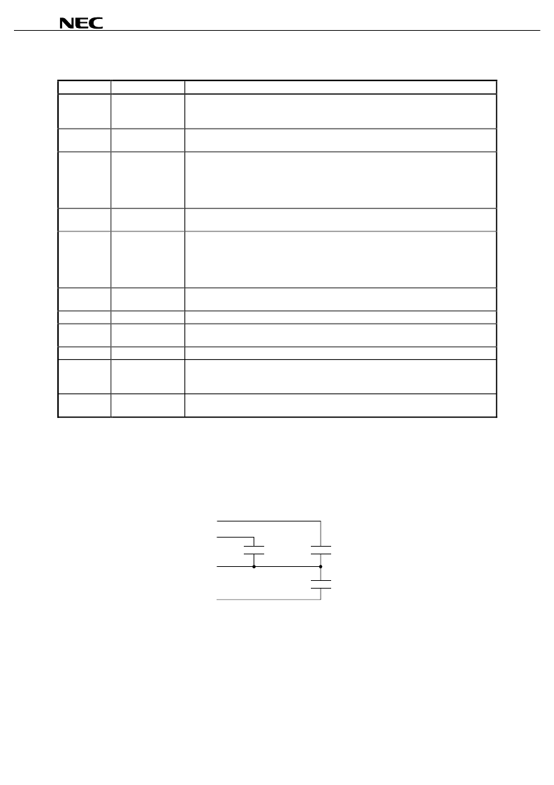
2. Insert a capacitor of about 0.1
μ
F between each power line, as shown below, to secure noise
margin such as V
IH
and V
IL
.
V
DD2
V
DD1
0.1
F
V
SS
V
EE1/2
μ
0.1
F
μ
0.1
F
μ
相關(guān)PDF資料 |
PDF描述 |
|---|---|
| UPD16700N | DUSTCAP, METAL SZ22; Material:Zinc Alloy; Colour:Nickel Plated; Connector shell size:22; Voltage rating, AC:750V; Series:TRIM TRIO |
| UPD16803 | MONOLITHIC DUAL H BRIDGE DRIVER CIRCUIT |
| UPD16803GS | MONOLITHIC DUAL H BRIDGE DRIVER CIRCUIT |
| UPD168103AK9-5B4-A | 5-CHANNEL OPERATIONAL AMPLIFIER, IRIS DRIVER, AND 4-CHANNEL H-BRIDGE DRIVER |
| UPD168103A | 5-CHANNEL OPERATIONAL AMPLIFIER, IRIS DRIVER, AND 4-CHANNEL H-BRIDGE DRIVER |
相關(guān)代理商/技術(shù)參數(shù) |
參數(shù)描述 |
|---|---|
| UPD16700N | 制造商:NEC 制造商全稱:NEC 功能描述:256-OUTPUT TFT-LCD GATE DRIVER |
| UPD16702 | 制造商:未知廠家 制造商全稱:未知廠家 功能描述:UPD16702 Data Sheet | Data Sheet[09/2001] |
| UPD16704 | 制造商:NEC 制造商全稱:NEC 功能描述:240-OUTPUT TFT-LCD GATE DRIVER |
| UPD16704P | 制造商:NEC 制造商全稱:NEC 功能描述:240-OUTPUT TFT-LCD GATE DRIVER |
| UPD16705 | 制造商:NEC 制造商全稱:NEC 功能描述:263/256-OUTPUT TFT-LCD GATE DRIVER |
發(fā)布緊急采購,3分鐘左右您將得到回復(fù)。