- 您現(xiàn)在的位置:買賣IC網(wǎng) > PDF目錄383979 > UPD16650N (NEC Corp.) 120-/128-OUTPUT TFT-LCD GATE DRIVER PDF資料下載
參數(shù)資料
| 型號: | UPD16650N |
| 廠商: | NEC Corp. |
| 英文描述: | 120-/128-OUTPUT TFT-LCD GATE DRIVER |
| 中文描述: | 120-/128-OUTPUT的TFT - LCD柵極驅(qū)動器 |
| 文件頁數(shù): | 4/12頁 |
| 文件大?。?/td> | 62K |
| 代理商: | UPD16650N |
μ
PD16650
4
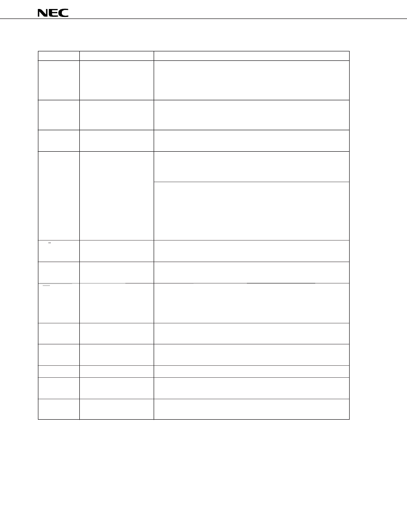
PIN DESCRIPTION
Pin symbol
Pin name
Description of function
Driver output
Output count change-over
input
Logic voltage change-over
input
Start pulse input/output
Shift direction change-over
input
Shift clock input
Output enable input
Driver positive supply volt-
age
Reference voltage
Ground
Driver negative supply volt-
age
Driver negative supply volt-
age
X
1
to X
128
MC
V
CHA
STVR
STVL
R/L
φ
X
OE
V
DD
V
CC
V
SS
V
EE1
V
EE2
Output scan signals to drive the TFT-LCD gate electrodes. The output changes
when the shift clock
φ
X
rises. The amplitude of the driver output is V
DD
- V
EE1
.
See the timing charts shown later for details of how to switch between the 120-
output mode and 128-output mode.
Receives a signal that changes the number of outputs. For the 120-output
mode, this pin must be supplied with a high level (V
CC
). For the 128-output
mode, it must be supplied with a low level (V
SS
or V
EE2
).
Must be supplied with the V
EE2
level when the logic supply voltage is 3.3 V, and
with the V
DD
level when the logic supply voltage is 5.0 V.
Receives an input to the internal shift register. The input data is loaded on the
shift register at the positive-going edge of the shift clock
φ
X
. The scan signals
are output from X
1
to X
128
. The input/output level is the CMOS level.
Outputs a start pulse to the next stage if a cascade connection is used. In the
120-output mode, the start pulse is output at the negative-going edge of the
120th shift clock
φ
X
pulse, and cleared at the negative-going edge of the 121st
pulse. In the 128-output mode, the start pulse is output at the negative-going
edge of the 128th shift clock
φ
X
pulse, and cleared at the negative-going edge
of the 129th pulse.
R/L = high (for shift right): STVR
→
X
1
→
X
128
→
STVL
R/L = low (for shift left)
: STVL
→
X
128
→
X
1
→
STVR
Receives a shift clock pulse for the internal shift register. A shift occurs at the
positive-going edge of the shift clock pulse.
When this pin is at a high level, the driver output is fixed at a low level. The
shift register is not cleared, however. The internal logic circuit operates even
when the pin is at a high level. The signal supplied to this pin is not
synchronized with the clock.
Receives the supply voltage for both the logic circuit and driver.
5
±
0.5 V/3.3
±
0.3 V
Reference voltage for the LS1 and LS2 level shifters.
Must be connected to the system ground.
V
EE1
(for the driver)
V
EE2
(for the logic circuit)
相關(guān)PDF資料 |
PDF描述 |
|---|---|
| UPD16655N-XXX | LCD Display Driver |
| UPD16655 | 240-OUTPUT TFT-LCD GATE DRIVER |
| UPD16655N | 240-OUTPUT TFT-LCD GATE DRIVER |
| UPD16664N-001 | 144/160/184/208-OUTPUT LCD COLUMN SEGMENT DRIVER WITH RAM |
| UPD16664N | RF CONNECTOR; 50 OHM REVERSE POLARITY BNC FEMALE BULKHEAD, CRIMP ATTACHMENT FOR RG58; *MEETS FCC PART 15.203 REQUIREMENTS* |
相關(guān)代理商/技術(shù)參數(shù) |
參數(shù)描述 |
|---|---|
| UPD16650N-XXX | 制造商:NEC 制造商全稱:NEC 功能描述:Interface IC |
| UPD16652N-XXX | 制造商:未知廠家 制造商全稱:未知廠家 功能描述:LCD Display Driver |
| UPD16654 | 制造商:NEC 制造商全稱:NEC 功能描述:150/154 OUTPUT TFT-LCD GATE DRIVE |
| UPD16654N | 制造商:NEC 制造商全稱:NEC 功能描述:150/154 OUTPUT TFT-LCD GATE DRIVE |
| UPD16655 | 制造商:NEC 制造商全稱:NEC 功能描述:240-OUTPUT TFT-LCD GATE DRIVER |
發(fā)布緊急采購,3分鐘左右您將得到回復(fù)。