- 您現在的位置:買賣IC網 > PDF目錄383979 > UPD16634AN-XXX (NEC Corp.) LCD Display Driver PDF資料下載
參數資料
| 型號: | UPD16634AN-XXX |
| 廠商: | NEC Corp. |
| 英文描述: | LCD Display Driver |
| 中文描述: | 液晶顯示驅動程序 |
| 文件頁數: | 6/20頁 |
| 文件大小: | 115K |
| 代理商: | UPD16634AN-XXX |
Data Sheet S12595EJ2V0DS00
6
μ
PD16634A
5. RELATIONHIP BETWEEN INPUT DATA AND OUTPUT VOLTAGE VALUE
This product incorporates a 6-bit D/A converter whose odd output pins and even output pins output respectively gray
scale voltages of differing polarity with respect to the LCD’s counter electrode (common electrode) voltage. The D/A
converter consists of ladder resistors and switches. The ladder resistors r
0
to r
62
are so designed that the ratios
between the LCD panel’s
γ
-corrected voltages and V
0
’ to V
63
’, V
0
” to V
63
” are roughly equal; and their respective
resistance values are as shown in Table 6-1. Among the 5-by 2
γ
-corrected voltages, input gray scale voltages of the
same polarity with respect to the common voltage, for the respective five
γ
-corrected voltages of V
0
to V
4
and V
5
to
V
9
. If fine gray scale voltage precision is not necessary, the voltage follower circuit supplied to the
γ
-corrected power
supplies V
1
to V
3
and V
6
to V
8
can be deleted.
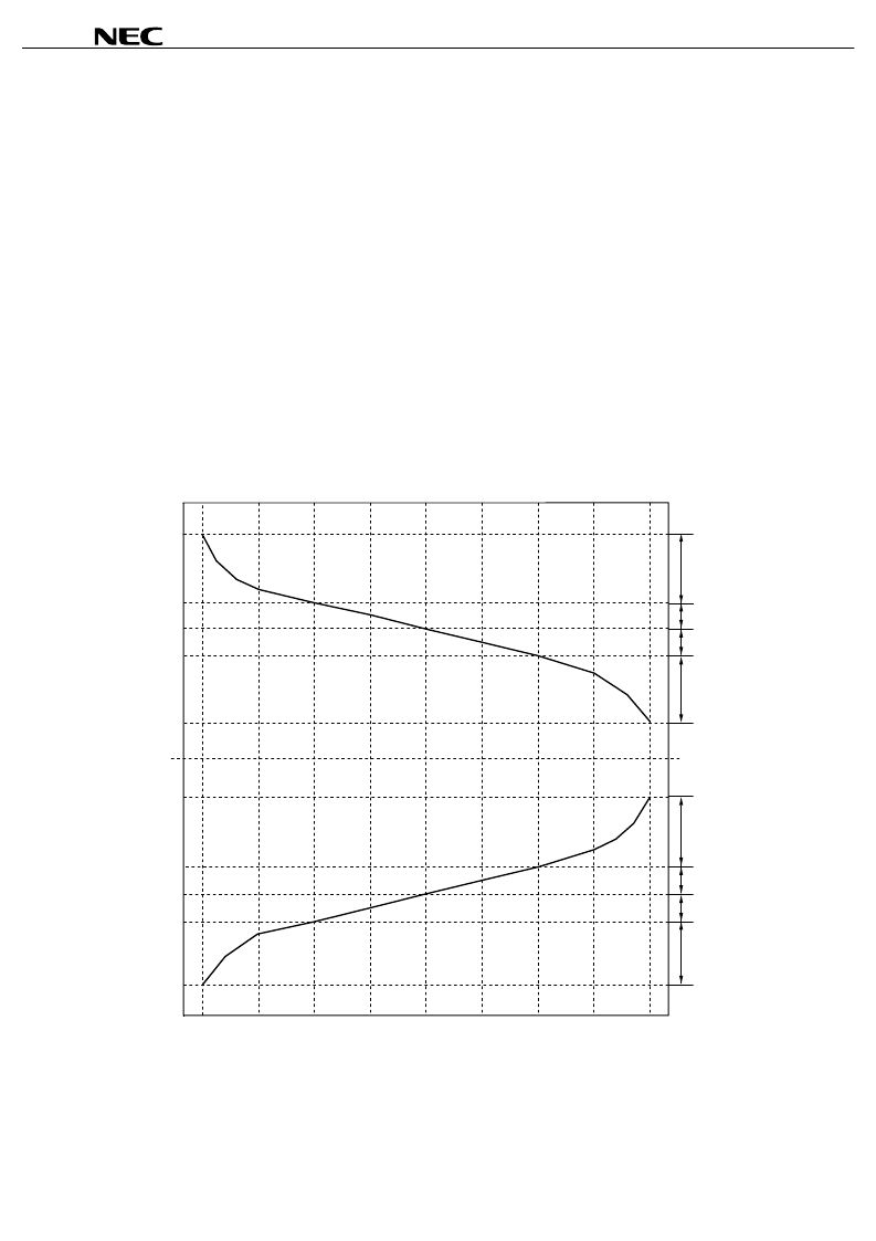
Figure 5-1 shows the relationship between the driving voltages such as liquid-crystal driving voltages V
DD2
and V
SS2
,
common electrode potential V
COM
, and
γ
-corrected voltages V
0
to V
9
and the input data. Be sure to maintain the
voltage relationships of V
DD2
> V
0
> V
1
> V
2
> V
3
> V
4
> V
5
> V
6
> V
7
> V
8
> V
9
> V
SS2
. Figure 6-1 and 6-2 show the
relationship between the input data and the output data.
This driver IC is designed for single-sided mounting. Therefore, please do not use it for
γ
-corrected power supply
level inversion in double-sided mounting.
Figure 5-1. Relationship between Input Data and Output Voltage
V
DD2
V
1
V
2
V
3
V
4
V
COM
V
5
V
6
V
7
V
8
V
SS2
00
08
10
18
20
28
30
38
Input data (HEX)
3F
16
16
16
15
15
16
16
16
Split interval
V
0
V
9
#
相關PDF資料 |
PDF描述 |
|---|---|
| UPD16634A | 300-OUTPUT TFT-LCD SOURCE DRIVER COMPATIBLE WITH 64 GRAY SCALE |
| UPD16634AN | 300-OUTPUT TFT-LCD SOURCE DRIVER COMPATIBLE WITH 64 GRAY SCALE |
| UPD16640C | 300/309-OUTPUT TFT-LCD SOURCE DRIVER 64 GRAY SCALE |
| UPD16640CN | 300/309-OUTPUT TFT-LCD SOURCE DRIVER 64 GRAY SCALE |
| UPD16641N-XXX | Interface IC |
相關代理商/技術參數 |
參數描述 |
|---|---|
| UPD16635 | 制造商:NEC 制造商全稱:NEC 功能描述:240-OUTPUT TFT-LCD SOURCE DRIVER |
| UPD16635N | 制造商:NEC 制造商全稱:NEC 功能描述:240-OUTPUT TFT-LCD SOURCE DRIVER |
| UPD16635N-XXX | 制造商:未知廠家 制造商全稱:未知廠家 功能描述:LCD Display Driver |
| UPD16636N-XXX | 制造商:未知廠家 制造商全稱:未知廠家 功能描述:LCD Display Driver |
| UPD16638AN | 制造商:未知廠家 制造商全稱:未知廠家 功能描述:LCD Display Driver |
發(fā)布緊急采購,3分鐘左右您將得到回復。