- 您現(xiàn)在的位置:買賣IC網 > PDF目錄384041 > UPD16435 (NEC Corp.) DOT MATRIX LCD CONTROLLER/DRIVER PDF資料下載
參數資料
| 型號: | UPD16435 |
| 廠商: | NEC Corp. |
| 英文描述: | DOT MATRIX LCD CONTROLLER/DRIVER |
| 中文描述: | 點陣LCD控制器/驅動 |
| 文件頁數: | 4/36頁 |
| 文件大?。?/td> | 310K |
| 代理商: | UPD16435 |
第1頁第2頁第3頁當前第4頁第5頁第6頁第7頁第8頁第9頁第10頁第11頁第12頁第13頁第14頁第15頁第16頁第17頁第18頁第19頁第20頁第21頁第22頁第23頁第24頁第25頁第26頁第27頁第28頁第29頁第30頁第31頁第32頁第33頁第34頁第35頁第36頁
μ
PD16435, 16435A
4
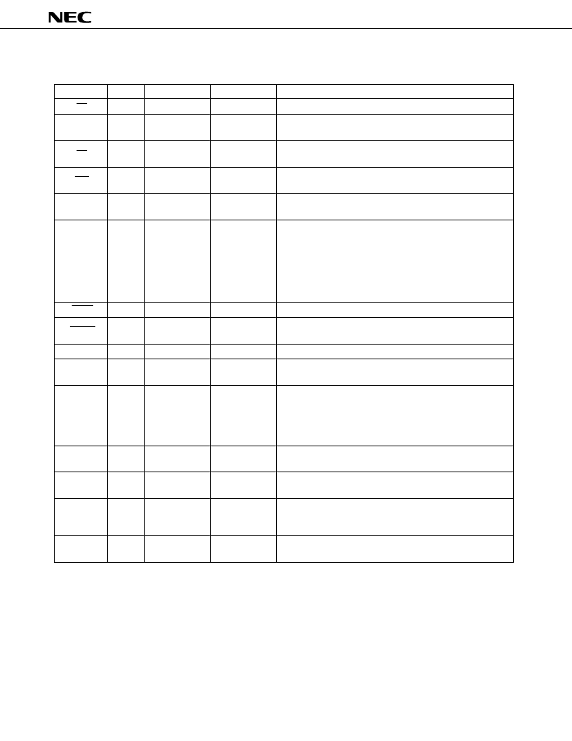
PIN DESCRIPTIONS
Description
Chip select signal
Register selection signal (specifies address register when “0”,
control register when “1”).
Read enable signal. Reads write address when scrolling.
Active edge is falling edge.
Write enable signal.
Active edge is falling edge.
Word length selection signal (4-bit input when “1”, 8-bit input
when “0”).
Transmit/receive data (3-state bidirectional)
Upper
→
D4 to D7
Lower
→
D0 to D3 (These pins should be set as unused in case
of 4-bit data).
In test mode, these pins are output pins.
In a 4-bit transfer, storage is performed in the upper (MSB) in
order from the data transferred first.
“0” indicates busy state.
“0”
→
Initialization of all internal registers and commands is
performed. Output is fixed at V
1
.
Signal is output to CPU on completion of one-character scroll.
Synchronization signal input/output pins for master/slave
operation.
μ
PD16435: Input the 4.19 MHz reference clock to the OSC
1
pin
externally. Leave the OSC
2
pin open. (Always outputs high
level.)
μ
PD16435A: This is the pin to which the 4.19 MHz crystal
resonator is connected. Input the external clock to OSC
1
first.
2 Hz external clock input pin. Scaled by 2 internally to generate 1
Hz, used as blink synchronization signal.
Common output signals
Segment output signals
“1”
→
Test mode
“0” or open
→
Normal operating mode
Output Type
–––
–––
–––
–––
–––
CMOS 3-state
Nch open-drain
–––
CMOS
Nch open-drain
–––
–––
Analog switch
Analog switch
–––
Input/Output
Input
Input
Input (Schmitt)
Input (Schmitt)
Input
Input/output
Output
Input
Output
Input/output
–––
Input (Schmitt)
Output
Output
Output
Pin Name
Pin No.
CS
RS
254
RD
253
WR
252
WS
251
250
to
243
D
0
to D
7
BUSY
240
RESET
242
SCR
241
SYNC
239
OSC
1
OSC
2
235
234
OSC
3
233
COM1 to
COM73
212 to 176
3 to 38
SEG1 to
SEG119
41 to 70
81 to 134
137 to 171
TEST1
TEST2
238
237
相關PDF資料 |
PDF描述 |
|---|---|
| UPD16435A | DOT MATRIX LCD CONTROLLER/DRIVER |
| UPD16654 | 150/154 OUTPUT TFT-LCD GATE DRIVE |
| UPD16654N | 150/154 OUTPUT TFT-LCD GATE DRIVE |
| UPD16676GF-3BA | 1/16, 1/32 DUTY LCD CONTROLLER/DRIVER |
| UPD16676 | 1/16, 1/32 DUTY LCD CONTROLLER/DRIVER |
相關代理商/技術參數 |
參數描述 |
|---|---|
| UPD16435A | 制造商:NEC 制造商全稱:NEC 功能描述:DOT MATRIX LCD CONTROLLER/DRIVER |
| UPD16435AN-001-001 | 制造商:NEC 制造商全稱:NEC 功能描述:DOT MATRIX LCD CONTROLLER/DRIVER |
| UPD16435AN-001-052 | 制造商:NEC 制造商全稱:NEC 功能描述:DOT MATRIX LCD CONTROLLER/DRIVER |
| UPD16435N-001-001 | 制造商:NEC 制造商全稱:NEC 功能描述:DOT MATRIX LCD CONTROLLER/DRIVER |
| UPD16435N-001-002 | 制造商:NEC 制造商全稱:NEC 功能描述:DOT MATRIX LCD CONTROLLER/DRIVER |
發(fā)布緊急采購,3分鐘左右您將得到回復。