- 您現(xiàn)在的位置:買賣IC網(wǎng) > PDF目錄384041 > UPD16334 (NEC Corp.) 96-Bit AC-PDP DRIVER PDF資料下載
參數(shù)資料
| 型號: | UPD16334 |
| 廠商: | NEC Corp. |
| 英文描述: | 96-Bit AC-PDP DRIVER |
| 中文描述: | 96位交流PDP驅(qū)動 |
| 文件頁數(shù): | 4/12頁 |
| 文件大小: | 97K |
| 代理商: | UPD16334 |
4
μ
PD16334
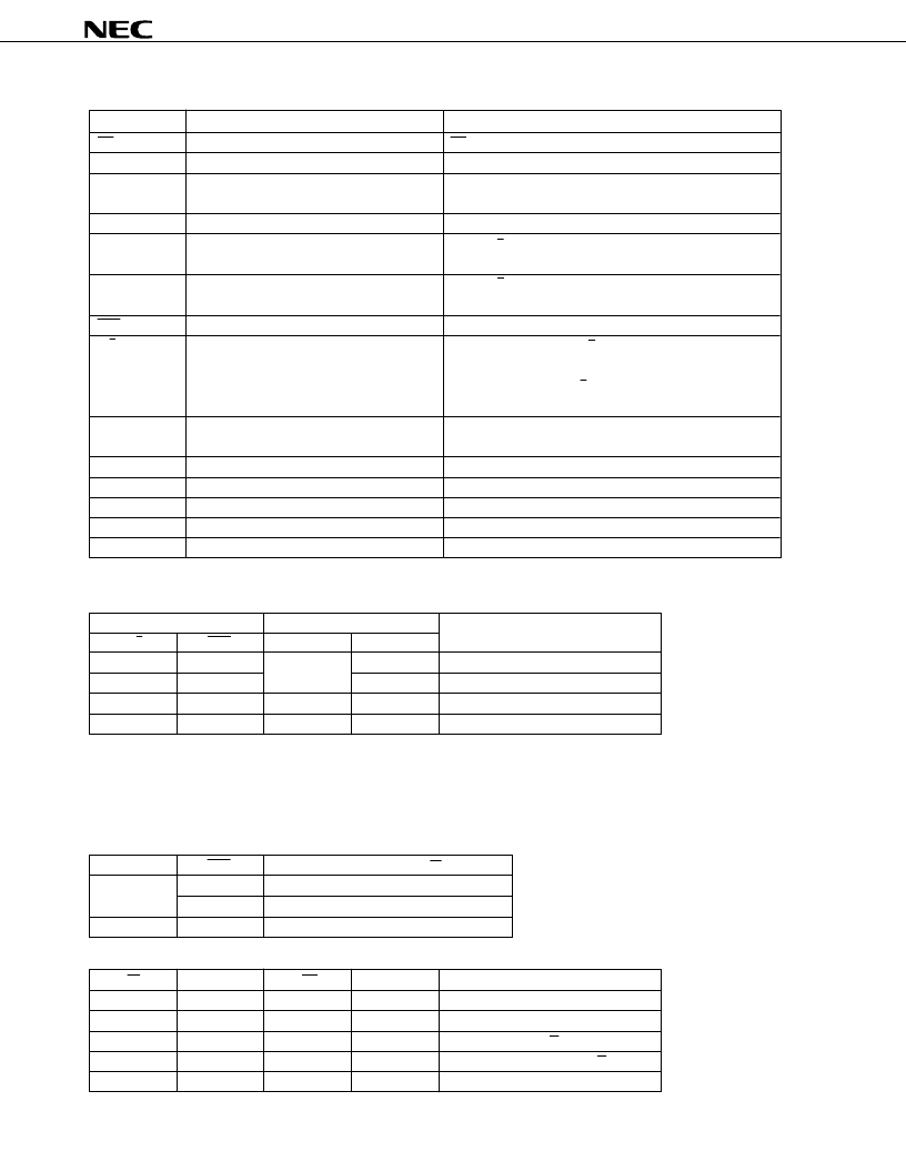
PIN DESCRIPTION
Symbol
Pin Name
Description
PC
Polarity change input
PC = L: All driver output invert
BLK
Blank input
BLK = H : All output = H or L
LE
Latch enable input
Automatically executes latch by setting high at rising edge
of the clock
OE
Output enable
Make output high impedance by input H
A
1
to A
3
(6)
RIGHT data input/output
(Note)
When R/L=H (values in parentheses are for 6-bit input)
A
1
to A
3 (6)
: Input B
1
to B
3 (6)
: Output
B
1
to B
3 (6)
LEFT data input/output
(Note)
When R/L=L (values in parentheses are for 6-bit input)
A
1
to A
3 (6)
: Output B
1
to B
3 (6)
: Input
CLK
Clock input
Shift executed on fall
R/L
Shift control input
Right shift mode when R/L= H
SR
1
: A1
→
S
1
...S
94
→
B1 (Same direction for SR
2
to SR
6
)
Left shift mode when R/L= L
SR
1
: B
1
→
S
94
...S
1
→
A
1
(Same direction for SR
2
to SR
6
)
H: 32-bit length shift register, 3-bit input
IBS
Input mode switch
L: 16-bit length shift register, 6-bit input
O
1
to O
96
High withstand voltage output
80 V, 50 mA
MAX.
5 V
±
10 %
10 to 70 V
V
DD1
Power supply for logic block
V
DD2
Power supply for driver block
V
SS1
Logic GND
Connect to system GND
V
SS2
Driver GND
Connect to system GND
Note
When input mode is 3-bit, set unused input and output pins “L” level.
TRUTH TABLE 1 (Shift Register Block)
Input
Output
Shift Register
R/L
CLK
↓
H or L
↓
H or L
A
B
H
Input
Output
Note1
Right shift execution
H
Output
Hold
L
Output
Note2
Input
Left shift execution
L
Output
Hold
Notes 1.
The data of S
91
to S
93
(S
85
to S
90
) shifts to S
94
to S
96
(S
91
to S
96
) and is output from B
1
to B
3
(B
1
to B
6
) at the falling
edge of the clock, respectively. (Values in parentheses are for 6-bit input)
2.
The data of S
4
to S
6
(S
7
to S
12
) shifts to S
1
to S
3
(S
1
to S
6
) and is output from A
1
to A
3
(A
1
to A
6
) at the falling
edge of the clock, respectively (Values in parentheses are for 6-bit input)
TRUTH TABLE 2 (Latch Block)
LE
CLK
↑
↓
X
Output State of Latch Block (L
n
)
H
Latch Sn data and hold output data
Hold latch data
L
Hold latch data
TRUTH TABLE 3 (Driver Block)
L
n
BLK
PC
OE
Output State of Driver Block
X
H
H
L
H (All driver outputs: H)
X
H
L
L
L (All driver outputs: L)
X
L
H
L
Output latch data (L
n
)
X
L
L
L
Output inverted latch data (L
n
)
X
X
X
H
Set output impedance high
X: H or L, H: High level, L: Low level
相關(guān)PDF資料 |
PDF描述 |
|---|---|
| UPD16335 | 96-Bit AC-PDP DRIVER |
| UPD16347 | 192-BIT AC-PDP DRIVER |
| UPD16435N-001-001 | DOT MATRIX LCD CONTROLLER/DRIVER |
| UPD16435AN-001-001 | DOT MATRIX LCD CONTROLLER/DRIVER |
| UPD16435N-001-002 | DOT MATRIX LCD CONTROLLER/DRIVER |
相關(guān)代理商/技術(shù)參數(shù) |
參數(shù)描述 |
|---|---|
| UPD16335 | 制造商:NEC 制造商全稱:NEC 功能描述:96-Bit AC-PDP DRIVER |
| UPD16337 | 制造商:NEC 制造商全稱:NEC 功能描述:64-BIT AC-PDP DRIVER |
| UPD16337GF-3BA | 制造商:NEC 制造商全稱:NEC 功能描述:64-BIT AC-PDP DRIVER |
| UPD16340 | 制造商:NEC 制造商全稱:NEC 功能描述:96-BIT AC-PDP DRIVER |
| UPD16341 | 制造商:NEC 制造商全稱:NEC 功能描述:96-BIT AC-PDP DRIVER |
發(fā)布緊急采購,3分鐘左右您將得到回復。