- 您現(xiàn)在的位置:買賣IC網(wǎng) > PDF目錄383977 > UPC1876 (NEC Corp.) US MTS DECODER PDF資料下載
參數(shù)資料
| 型號: | UPC1876 |
| 廠商: | NEC Corp. |
| 英文描述: | US MTS DECODER |
| 中文描述: | 美國的多邊貿(mào)易體制解碼器 |
| 文件頁數(shù): | 24/40頁 |
| 文件大小: | 309K |
| 代理商: | UPC1876 |
第1頁第2頁第3頁第4頁第5頁第6頁第7頁第8頁第9頁第10頁第11頁第12頁第13頁第14頁第15頁第16頁第17頁第18頁第19頁第20頁第21頁第22頁第23頁當前第24頁第25頁第26頁第27頁第28頁第29頁第30頁第31頁第32頁第33頁第34頁第35頁第36頁第37頁第38頁第39頁第40頁
μ
PC1876
24
Data Sheet S11666EJ4V0DS00
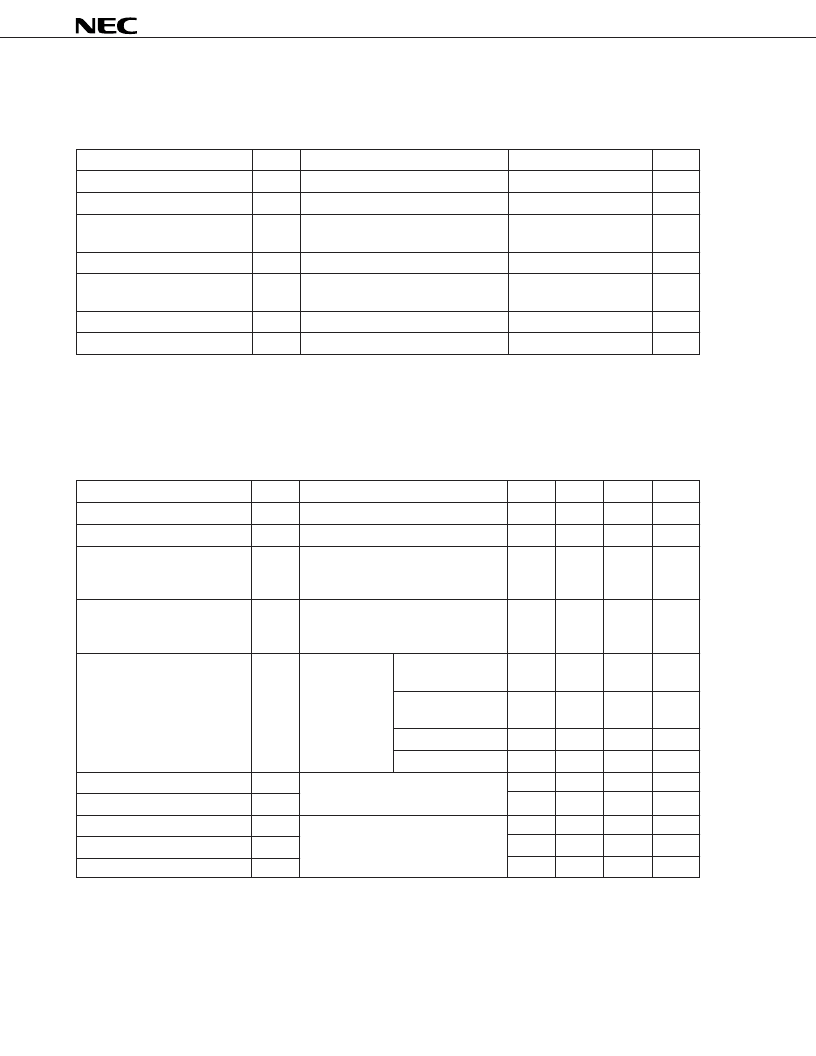
6. ELECTRICAL SPECIFICATIONS
Absolute Maximum Ratings (T
A
= +25C)
Parameter
Symbol
Conditions
Ratings
Unit
Supply voltage
V
CC
11
V
LED driver current
I
D
Current fed into SAPL and STL pins
30
mA
Control pin voltage
V
cont
Voltage applied to fHSW, SAP1/2,
ST/SAP, MUTE and FMONO pins
V
CC
+ 0.2
V
Input signal voltage
V
in
Voltage applied to COM pin
V
CC
V
Power dissipation
P
D
T
A
= 75C, in using the Universal
(10
×
10 cm
2
) Glass Epoxy Board
500
mW
Operating ambient temperature
T
A
V
CC
= 9 V
–20 to +75
C
Storage temperature
T
stg
–40 to +125
C
Caution If any of the parameters exceeds the absolute maximum ratings, even momentarily, the device
reliability may be impaired. The absolute maximum ratings are values that may physically damage
the product. Be sure to use the product within the ratings.
Recommended Operating Conditions
Parameter
Symbol
Conditions
MIN.
TYP.
MAX.
Unit
Supply voltage
V
CC
8.0
9.0
10.0
V
LED driver current
I
D
Current fed into SAPL and STL pins
25
mA
Output load impedance 1
R
L1
A.C. load impedance which can drive
output from ROT and LOT pins.
(at 100% modulation)
2
k
Output load impedance 2
R
L2
A.C. load impedance which can drive
output from SOT pin.
(at 100% modulation)
10
k
Input signal voltage
V
in
Signal voltage
applied to COM
L + R signal
(100% modulation)
0.424
V
p-p
pin
L – R signal
(100% modulation)
0.848
V
p-p
Pilot signal
0.0848
V
p-p
SAP signal
0.254
V
p-p
Control pin voltage 1 (High)
V
contH1
SAP1/2, ST/SAP and MUTE pins
3.5
V
CC
V
Control pin voltage 1 (Low)
V
contL1
0
0.8
V
Control pin voltage 2 (High)
V
contH2
FMONO pin
3.5
V
CC
V
Control pin voltage 2 (Mid.)
V
contM2
1.5
2.5
V
Control pin voltage 2 (Low)
V
contL2
0
0.8
V
相關(guān)PDF資料 |
PDF描述 |
|---|---|
| UPC2533GS-01 | AM TUNER FOR ELECTRONIC TUNING CAR RADIOS |
| UPC2533GS-02 | AM TUNER FOR ELECTRONIC TUNING CAR RADIOS |
| UPC2533 | AM TUNER FOR ELECTRONIC TUNING CAR RADIOS |
| UPC2539GS | DIODE ZENER DUAL ISOLATED 200mW 6Vz 20mA-Izt 0.05 5uA-Ir 3.5 SOT-363 3K/REEL |
| UPC2539 | CONN RCPT MALE 35POS WALL MT |
相關(guān)代理商/技術(shù)參數(shù) |
參數(shù)描述 |
|---|---|
| UPC1876GT | 制造商:NEC 制造商全稱:NEC 功能描述:US MTS DECODER |
| UPC1883 | 制造商:Panasonic Industrial Company 功能描述:IC |
| UPC1883CT | 制造商:Panasonic Industrial Company 功能描述:IC |
| UPC1884 | 制造商:NEC 制造商全稱:NEC 功能描述:SYNC SIGNAL PROCESSOR FOR MULTI-SYNC DISPLAY |
| UPC1888FCT | 制造商:Renesas Electronics Corporation 功能描述: |
發(fā)布緊急采購,3分鐘左右您將得到回復(fù)。