- 您現(xiàn)在的位置:買賣IC網(wǎng) > PDF目錄383976 > UPC1555G2 (NEC Corp.) TIMER CIRCUIT PDF資料下載
參數(shù)資料
| 型號: | UPC1555G2 |
| 廠商: | NEC Corp. |
| 英文描述: | TIMER CIRCUIT |
| 中文描述: | 定時器電路 |
| 文件頁數(shù): | 7/12頁 |
| 文件大小: | 103K |
| 代理商: | UPC1555G2 |
7
μ
PC1555
APPLICATION CIRCUITS
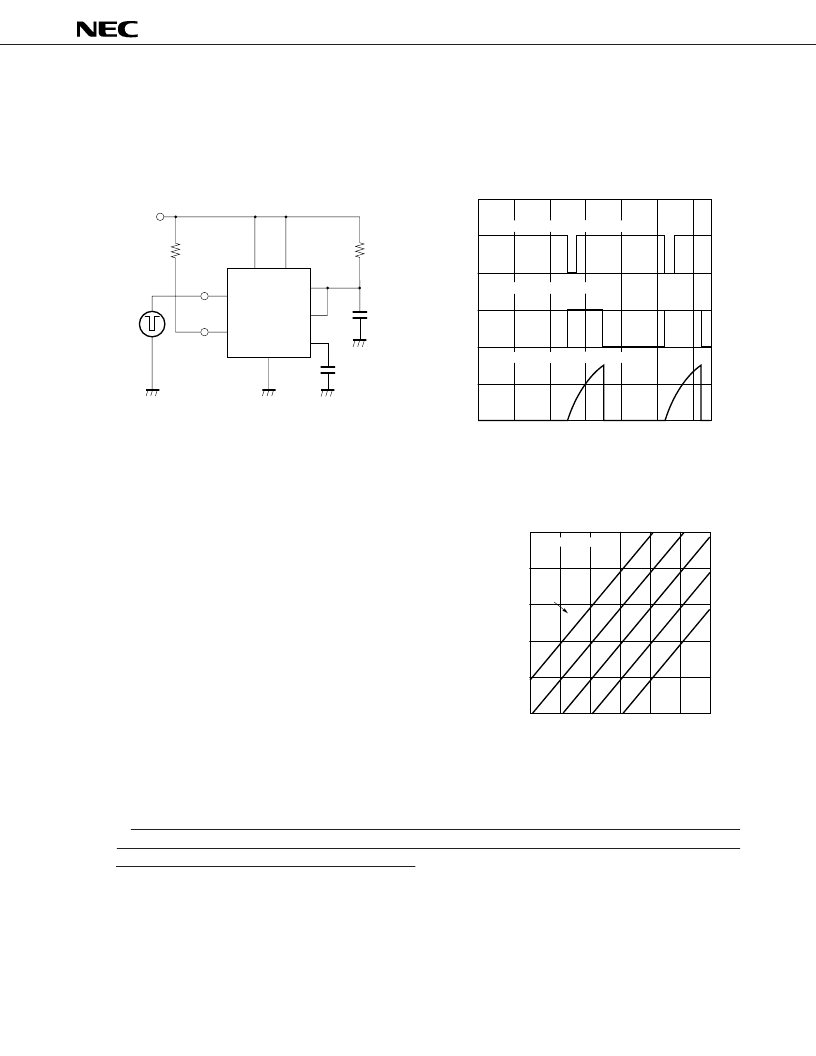
(1) Monostable multivibrator
Fig. a Monostable Multivibrator Example
Fig. b Monostable Response Waveform
Fig. c Interrelationships among Output
Pulse Width, R
1
, and C
1
(approxi-
mate value obtained by calculation)
When the
μ
PC1555 is configured as shown in
Fig. a, it functions as a monostable multivibrator.
Applying a voltage one-third as high as V
CC
or less
(trigger pulse
Note 9
) to pin 2 (trigger pin) drives the
output to a high level. Under this condition, capacitor
C
1
starts charging through resistor R
1
. When C
1
is
charged up to two-thirds as high as V
CC
, pin 6 (threshold
pin) is turned on and inverted to a low level. At this point,
C
1
starts discharging through pin 7. When a trigger
pulse is applied to pin 2 again, the same operation is
repeated. Fig. b shows this operation. A capacitor
connected to pin 5 functions as a nose filter for the
control voltage. If pin 4 (reset pin) is connected to 1 V
or higher (for example, by being connected to V
CC
), the
circuit operation can be stopped by switching it from 2
V or higher to a GND level.
The output pulse width (delay) is determined theo-
retically by (see Fig. c):
t = 1.1
C
1
R
1
The value obtained by this equation is only an approximate value, however. If it is necessary to obtain an accurate
output pulse width, determine R
1
and C
1
through actual measurement and confirmation; a trimmer should be used
as required. Moreover, R
1
should be 300
or higher.
Notes
9.
Keep the trigger pulse width smaller than the output pulse width.
10.
If the load is connected across the output and GND pins, a “staircase” occurs in the output waveform.
The application circuits and their parameters are for references only and are not intended for use in actual
design-in's.
OUTPUT
TRIGGER
3
2
4
8
7
6
5
1
R
L
V
CC
= 5 to 15 V
R
1
C
1
Control voltage
0.01 F
PC1555
μ
Note 10
"H"
"L"
"L"
"H"
(R
1
= 9.1 k
, C
1
= 0.01 F, R
L
= 1 k
)
t = 0.1 ms/DIV
Trigger input voltage: 5 V/DIV
Output voltage: 5 V/DIV
Capacitor (C
1
) voltage: 2 V/DIV
μ
μ
10k
1
10k
1M
1 M
100
10
10
s
100
s
1.0
ms
10
ms
100
ms
1.0
s
10
s
1.0
0.1
0.01
0.001
t = 1.1 C
1
R
1
(R
1
)
μ
C
1
Output pulse width t
相關(guān)PDF資料 |
PDF描述 |
|---|---|
| UPC1652G | SILICON MONOLITHIC BIPOLAR INTEGRATED CIRCUIT WIDE BAND AMPLIFIER |
| UPC1654 | 1.0 GHz SILICON MMIC AMPLIFIER |
| UPC1656 | 850 MHz WIDE-BAND SILICON MMIC AMPLIFIER |
| UPC1663G | ULTRA-WIDEBAND DIFFERENTIAL VIDEO AMPLIFIER |
| UPC1668C | HIGH ISOLATION SILICON MMIC IF AMPLIFIER |
相關(guān)代理商/技術(shù)參數(shù) |
參數(shù)描述 |
|---|---|
| UPC1555G2-A | 制造商:Renesas Electronics 功能描述:Cut Tape 制造商:Renesas 功能描述:Standard Timer Single 8-Pin SOP |
| UPC156 | 制造商:未知廠家 制造商全稱:未知廠家 功能描述: |
| UPC156A | 制造商:未知廠家 制造商全稱:未知廠家 功能描述:INDUSTRIAL LINEAR ICS |
| UPC157 | 制造商:未知廠家 制造商全稱:未知廠家 功能描述: |
| UPC1571C | 制造商:Panasonic Industrial Company 功能描述:IC |
發(fā)布緊急采購,3分鐘左右您將得到回復(fù)。