- 您現(xiàn)在的位置:買賣IC網(wǎng) > PDF目錄383975 > UPB587G-E1 (NEC Corp.) 1.0 GHz DIVIDE- BY- 2/4/8 PRESCALER PDF資料下載
參數(shù)資料
| 型號: | UPB587G-E1 |
| 廠商: | NEC Corp. |
| 英文描述: | 1.0 GHz DIVIDE- BY- 2/4/8 PRESCALER |
| 中文描述: | 1.0 GHz的分頻2/4/8預(yù)分頻器 |
| 文件頁數(shù): | 2/5頁 |
| 文件大小: | 124K |
| 代理商: | UPB587G-E1 |
ABSOLUTE MAXIMUM RATINGS
1
(T
A
= 25
°
C)
SYMBOLS
PARAMETERS
UNITS
RATINGS
V
CC1,
V
CC2
Supply Voltage
V
IN,
V
M
Input Voltage,
Ratio Control Voltage
P
IN
Input Power
P
T
Power Dissipation
V
-0.5 to 4.0
V
-0.5 to V
CC
+ 0.5
+10
dBm
UPB587B
UPB587G
W
mW
1.5 (T
A
= +125
°
C)
250 (T
A
= +85
°
C)
T
OP
Operating Temperature
UPB587B
UPB587G
Storage Temperature
UPB587B
UPB587G
°
C
°
C
-55 to +125
-40 to +85
T
STG
°
C
°
C
-65 to +200
-65 to +150
UPB587B, UPB587G
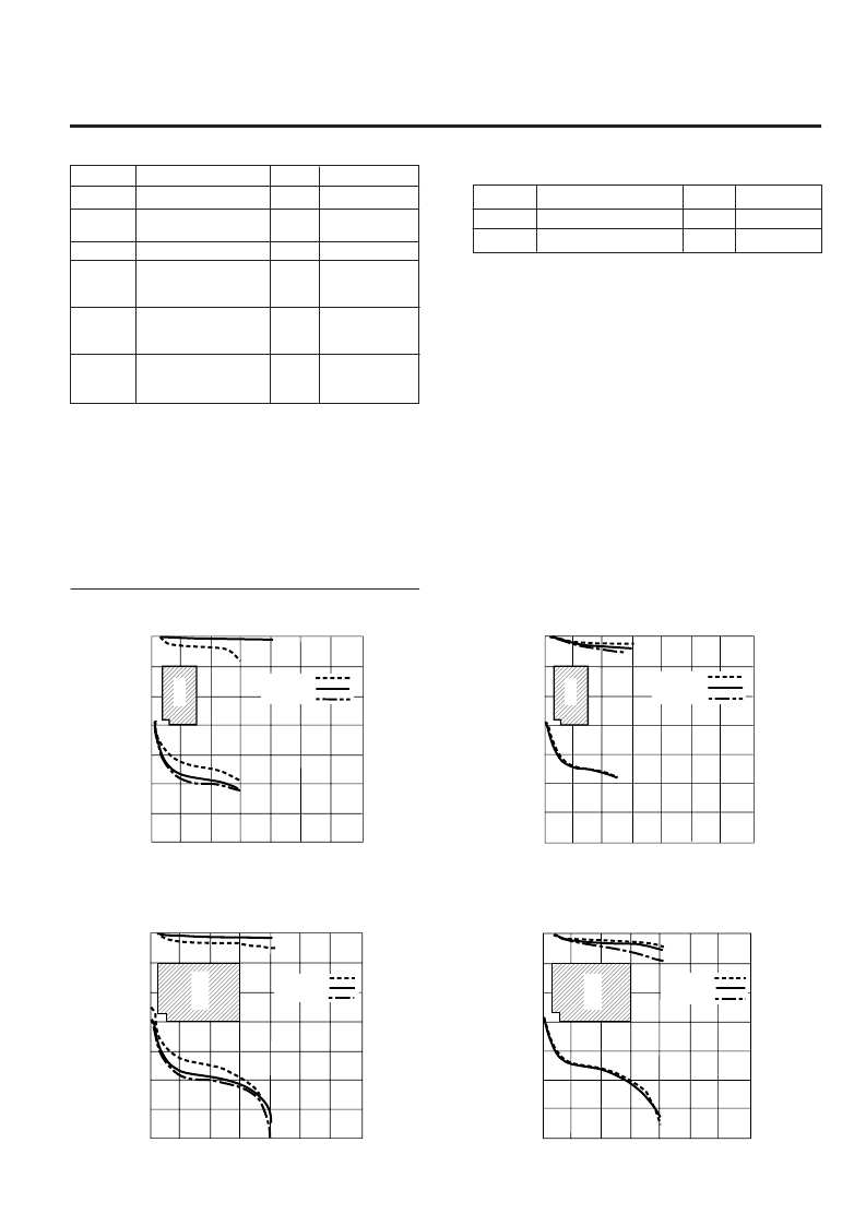
FREQUENCY RESPONSE
(DIVIDE-BY-2 @ T
A
= 25
°
C)
Frequency, f (GHz)
Frequency, f (GHz)
FREQUENCY RESPONSE
(DIVIDE-BY-2 @ V
CC
= 2.2 V)
SYMBOL
PARAMETER
UNITS
RATINGS
V
CC1,
V
CC2
Supply Voltage
V
2.2 to 3.5
T
OP
Operating Temperature
°
C
-20 to +75
RECOMMENDED
OPERATING CONDITIONS
Note: Because of the high internal gain and gain compression of the
UPB587, this device is prone to self-oscillation in the absence of an RF
input signal. If the device will be used in an application where DC power
will be applied in the absence of an RF input signal, this self-oscillation
can be suppressed by any of the following means:
*
Add a shunt resistor from the RF input line to ground. The
blocking capacitor should be between the resistor and the
UPB587, but physical separation should be minimized. Typically a
resistor value between 50 and 100 ohms will suppress the self-
oscillation.
*
Apply a DC offset voltage of +2.0 volts to the INPUT pin. The
voltage source should be isolated from the INPUT pin by a series
1000 ohm resistor.
*
Apply a DC offset voltage of +1.0 volts to the BYPASS pin. The
voltage source should be isolated from the BYPASS pin by a
series 1000 ohm resistor.
All these approaches reduce the input sensitivity of the UPB587 (by as
much as 3 dB for the example of a 50 ohm shunt resistor), but otherwise
have no affect on the reliability or other electrical characteristics of this
device.
Frequency, f (GHz)
FREQUENCY RESPONSE
(DIVIDE-BY-4 @ T
A
= 25
°
C)
Frequency, f (GHz)
FREQUENCY RESPONSE
(DIVIDE-BY-4 @ V
CC
= 2.2 V)
Guaranteed
Operating
Window
*
TYPICAL PERFORMANCE CURVES
(T
A
= 25
°
C unless otherwise noted)
I
I
(
I
I
(
I
I
(
I
I
(
Note:
1. Operation in excess of any one of these parameters may result in
permanent damage.
V
CC
= 2.2 V
3.0 V
3.5 V
+10
0
-10
-20
-30
-40
-50
-60
0 0.2 0.4 0.6 0.8 1.0 1.2 1.4
G*
O
W
10
0
-10
-20
-30
-40
-50
-60
0 0.2 0.4 0.6 0.8 1.0 1.2 1.4
T
A
= +75C
+25C
-20C
G*
O
W
+10
0
-10
-20
-30
-40
-50
-60
0 0.2 0.4 0.6 0.8 1.0 1.2 1.4
V
CC
= 2.2 V
3.0 V
3.5 V
G
*
O
W
TA = +75C
+25C
-20C
+10
0
-10
-20
-30
-40
-50
-60
0 0.2 0.4 0.6 0.8 1.0 1.2 1.4
G
*
O
W
相關(guān)PDF資料 |
PDF描述 |
|---|---|
| UPB8284A | CLOCK GENERATOR AND DRIVER FOR 8086/8088 MICROPROCESSORS |
| UPC1060 | CONNECTOR ACCESSORY |
| UPC1060C | CONNECTOR ACCESSORY |
| UPC1093 | CONNECTOR ACCESSORY |
| UPC1093G | CONNECTOR ACCESSORY |
相關(guān)代理商/技術(shù)參數(shù) |
參數(shù)描述 |
|---|---|
| UPB587P | 制造商:未知廠家 制造商全稱:未知廠家 功能描述:Analog IC |
| UPB588B | 制造商:未知廠家 制造商全稱:未知廠家 功能描述:Prescaler/Frequency Divider |
| UPB588G | 制造商:Panasonic Industrial Company 功能描述:IC |
| UPB588P | 制造商:未知廠家 制造商全稱:未知廠家 功能描述:Analog IC |
| UPB595CX | 制造商:未知廠家 制造商全稱:未知廠家 功能描述:Prescaler/Frequency Divider |
發(fā)布緊急采購,3分鐘左右您將得到回復(fù)。