- 您現(xiàn)在的位置:買賣IC網(wǎng) > PDF目錄383974 > UPA1902 (NEC Corp.) N-CHANNEL MOS FIELD EFFECT TRANSISTOR FOR SWITCHING PDF資料下載
參數(shù)資料
| 型號: | UPA1902 |
| 廠商: | NEC Corp. |
| 英文描述: | N-CHANNEL MOS FIELD EFFECT TRANSISTOR FOR SWITCHING |
| 中文描述: | N溝道MOS場效應(yīng)晶體管開關(guān) |
| 文件頁數(shù): | 1/6頁 |
| 文件大?。?/td> | 132K |
| 代理商: | UPA1902 |
The information in this document is subject to change without notice. Before using this document, please
confirm that this is the latest version.
Not all products and/or types are available in every country. Please check with an NEC Electronics
sales representative for availability and additional information.
2003
MOS FIELD EFFECT TRANSISTOR
μ
PA1902
N-CHANNEL MOS FIELD EFFECT TRANSISTOR
FOR SWITCHING
DATA SHEET
Document No. G16634EJ1V0DS00 (1st edition)
Date Published October 2003 NS CP(K)
Printed in Japan
DESCRIPTION
The
μ
PA1902 is a switching device, which can be driven
directly by a 4.5 V power source.
This
μ
PA1902 features a low on-state resistance and excellent
switching characteristics, and is suitable for applications such as
power management switch of portable machine and so on.
FEATURES
4.5 V drive available
Low on-state resistance
R
DS(on)1
= 17 m
TYP. (V
GS
= 10 V, I
D
= 3.5 A)
R
DS(on)2
= 22 m
TYP. (V
GS
= 4.5 V, I
D
= 3.5 A)
ORDERING INFORMATION
PART NUMBER
PACKAGE
μ
PA1902TE
SC-95 (Mini Mold Thin Type)
Marking: TY
ABSOLUTE MAXIMUM RATINGS (T
A
= 25°C)
Drain to Source Voltage (V
GS
= 0 V)
Gate to Source Voltage (V
DS
= 0 V)
Drain Current (DC)
Drain Current (pulse)
Note1
Total Power Dissipation
Total Power Dissipation
Note2
Channel Temperature
Storage Temperature
Notes 1.
PW
≤
10
μ
s, Duty Cycle
≤
1%
2.
Mounted on FR-4 board of 50 mm x 50 mm x 1.6 mm, t
≤
5
sec.
Remark
Strong electric field, when exposed to this device, can cause destruction of the gate oxide and ultimately
degrade the device operation. Steps must be taken to stop generation of static electricity as much as
possible, and quickly dissipate it once, when it has occurred.
Caution
This product is electrostatic-sensitive device due to low ESD capability and should be handled with
caution for electrostatic discharge. (It does not have built-in G-S protection diode.)
When this product actually used, an additional protection circuit is externally required if a voltage
exceeding the rated voltage may be applied to this device.
V
DSS
V
GSS
I
D(DC)
I
D(pulse)
P
T1
P
T2
T
ch
T
stg
30
±
20
±
7.0
±
28
0.2
2.0
150
V
V
A
A
W
W
°C
°C
55 to +150
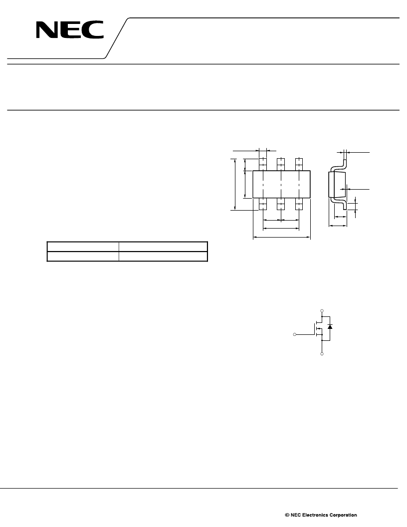
PACKAGE DRAWING (Unit: mm)
0.65
0.9 to 1.1
0 to 0.1
0.16
+0.1
0
2
1
0.95
1.9
2.9 ±0.2
0.32
+0.1
0.95
0
+
–
1
2
3
6
5
4
1, 2, 5, 6: Drain
3
4
: Gate
: Source
EQUIVALENT CIRCUIT
Drain
Source
Body
Diode
Gate
相關(guān)PDF資料 |
PDF描述 |
|---|---|
| UPA1902TE | N-CHANNEL MOS FIELD EFFECT TRANSISTOR FOR SWITCHING |
| UPA1910 | P-CHANNEL MOS FIELD EFFECT TRANSISTOR FOR SWITCHING |
| UPA1910TE | P-CHANNEL MOS FIELD EFFECT TRANSISTOR FOR SWITCHING |
| UPA1911A | P-CHANNEL MOS FIELD EFFECT TRANSISTOR FOR SWITCHING |
| UPA1911ATE | P-CHANNEL MOS FIELD EFFECT TRANSISTOR FOR SWITCHING |
相關(guān)代理商/技術(shù)參數(shù) |
參數(shù)描述 |
|---|---|
| UPA1902TE | 制造商:NEC 制造商全稱:NEC 功能描述:N-CHANNEL MOS FIELD EFFECT TRANSISTOR FOR SWITCHING |
| UPA1902TE-T1-A | 制造商:Renesas Electronics 功能描述:Trans MOSFET N-CH 30V 7A 6-Pin SC-95 T/R Cut Tape 制造商:Renesas 功能描述:Trans MOSFET N-CH 30V 7A 6-Pin SC-95 T/R |
| UPA1910 | 制造商:NEC 制造商全稱:NEC 功能描述:P-CHANNEL MOS FIELD EFFECT TRANSISTOR FOR SWITCHING |
| UPA1910TE | 制造商:NEC 制造商全稱:NEC 功能描述:P-CHANNEL MOS FIELD EFFECT TRANSISTOR FOR SWITCHING |
| UPA1911 | 制造商:NEC 制造商全稱:NEC 功能描述:P-CHANNEL MOS FIELD EFFECT TRANSISTOR FOR SWITCHING |
發(fā)布緊急采購,3分鐘左右您將得到回復(fù)。