- 您現(xiàn)在的位置:買賣IC網(wǎng) > PDF目錄383974 > UPA1815GR-9JG (NEC Corp.) P-CHANNEL MOS FIELD EFFECT TRANSISTOR FOR SWITCHING PDF資料下載
參數(shù)資料
| 型號: | UPA1815GR-9JG |
| 廠商: | NEC Corp. |
| 英文描述: | P-CHANNEL MOS FIELD EFFECT TRANSISTOR FOR SWITCHING |
| 中文描述: | P溝道MOS場效應(yīng)晶體管開關(guān) |
| 文件頁數(shù): | 1/8頁 |
| 文件大小: | 68K |
| 代理商: | UPA1815GR-9JG |
The information in this document is subject to change without notice. Before using this document, please
confirm that this is the latest version.
Not all devices/types available in every country. Please check with local NEC representative for
availability and additional information.
1998, 1999
MOS FIELD EFFECT TRANSISTOR
μ
PA1815
P-CHANNEL MOS FIELD EFFECT TRANSISTOR
FOR SWITCHING
DATA SHEET
Document No.
Date Published
Printed in Japan
D13805EJ2V0DS00 (2nd edition)
August 1999 NS CP(K)
The mark
#
shows major revised points.
DESCRIPTION
The
μ
PA1815 is a switching device which can be
driven directly by a 2.5-V power source.
The
μ
PA1815 features a low on-state resistance and
excellent switching characteristics, and is suitable for
applications such as power switch of portable machine
and so on.
FEATURES
Can be driven by a 2.5-V power source
Low on-state resistance
R
DS(on)1
= 15 m
MAX. (V
GS
= –4.5 V, I
D
= –3.5 A)
R
DS(on)2
= 16 m
MAX. (V
GS
= –4.0 V, I
D
= –3.5 A)
R
DS(on)3
= 19 m
MAX. (V
GS
= –3.3 V, I
D
= –3.5 A)
R
DS(on)4
= 23 m
MAX. (V
GS
= –2.5 V, I
D
= –3.5 A)
ORDERING INFORMATION
PART NUMBER
PACKAGE
μ
PA1815GR-9JG
Power TSSOP8
ABSOLUTE MAXIMUM RATINGS (T
A
= 25°C)
Drain to Source Voltage
V
DSS
–20
V
Gate to Source Voltage
V
GSS
±12
V
Drain Current (DC)
Drain Current (pulse)
Note1
Total Power Dissipation
Note2
I
D(DC)
±7
A
I
D(pulse)
±26
A
P
T
2.0
W
Channel Temperature
T
ch
150
°C
Storage Temperature
T
stg
–55 to +150
°C
Notes 1.
PW
≤
10
μ
s, Duty Cycle
≤
1
%
2.
Mounted on ceramic substrate of 5000
mm
2
x 1.1
mm
Remark
The diode connected between the gate and source of the transistor serves as a protector against ESD.
When this device actually used, an additional protection circuit is externally required if a voltage
exceeding the rated voltage may be applied to this device.
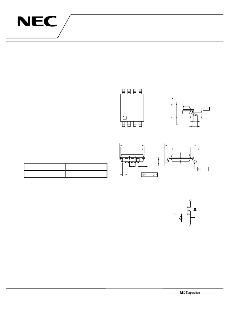
PACKAGE DRAWING (Unit : mm)
1
4
8
5
6.4 ±0.2
4.4 ±0.1
1.0 ±0.2
0
±
0.1
1, 5, 8
2, 3, 6, 7:Source
4
:Drain
:Gate
0.8 MAX.
3.15 ±0.15
3.0 ±0.1
0.65
0.10 M
0.27
+0.03
0.25
0.5
0.6
+0.15
3
°
+5
°
–3
°
1.2 MAX.
1.0±0.05
0.1±0.05
EQUIVALENT CIRCUIT
Source
Body
Diode
Gate
Protection
Diode
Gate
Drain
#
相關(guān)PDF資料 |
PDF描述 |
|---|---|
| UPA1815 | P-CHANNEL MOS FIELD EFFECT TRANSISTOR FOR SWITCHING |
| UPA1818GR-9JG | P-CHANNEL MOS FIELD EFFECT TRANSISTOR FOR SWITCHING |
| UPA1852GR-9JG | N-CHANNEL MOS FIELD EFFECT TRANSISTOR FOR SWITCHING |
| UPA1852 | CODING RING, RECEPTACLE YELLOW; Colour:Yellow; Connector shell size:10 |
| UPA1853 | P-CHANNEL MOS FIELD EFFECT TRANSISTOR FOR SWITCHING |
相關(guān)代理商/技術(shù)參數(shù) |
參數(shù)描述 |
|---|---|
| UPA1816 | 制造商:NEC 制造商全稱:NEC 功能描述:P-CHANNEL MOS FIELD EFFECT TRANSISTOR FOR SWITCHING |
| UPA1816GR-9JG | 制造商:NEC 制造商全稱:NEC 功能描述:P-CHANNEL MOS FIELD EFFECT TRANSISTOR FOR SWITCHING |
| UPA1817 | 制造商:NEC 制造商全稱:NEC 功能描述:P-CHANNEL MOS FIELD EFFECT TRANSISTOR FOR SWITCHING |
| UPA1817GR-9JG | 制造商:NEC 制造商全稱:NEC 功能描述:P-CHANNEL MOS FIELD EFFECT TRANSISTOR FOR SWITCHING |
| UPA1817GR-9JG-E1 | 制造商:Renesas Electronics Corporation 功能描述: |
發(fā)布緊急采購,3分鐘左右您將得到回復(fù)。