- 您現(xiàn)在的位置:買賣IC網(wǎng) > PDF目錄359308 > UC3844TD (意法半導(dǎo)體) HIGH PERFORMANCE CURRENT MODE PWM CONTROLLER PDF資料下載
參數(shù)資料
| 型號: | UC3844TD |
| 廠商: | 意法半導(dǎo)體 |
| 英文描述: | HIGH PERFORMANCE CURRENT MODE PWM CONTROLLER |
| 中文描述: | 高性能電流模式PWM控制器 |
| 文件頁數(shù): | 2/15頁 |
| 文件大小: | 228K |
| 代理商: | UC3844TD |
* All voltages are with respect to pin 5, all currents are positive into the specified terminal.
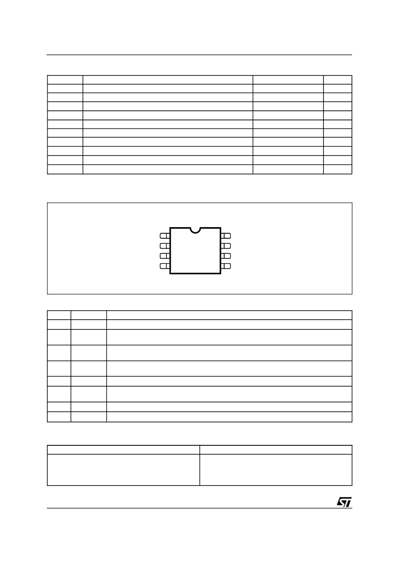
PIN CONNECTION
(top view)
COMP
V
FB
I
SENSE
R
T
/C
T
GROUND
OUTPUT
Vi
V
REF
1
3
2
4
6
5
7
8
D95IN332
Minidip/SO8
ORDERING NUMBERS
SO8
Minidip
UC3842TN
UC3843TN
UC3844TN
UC3845TN
UC3842TD
UC3843TD
UC3844TD
UC3845TD
ABSOLUTE MAXIMUM RATINGS
Symbol
V
i
V
i
I
O
E
O
Parameter
Value
30
Self Limiting
±
1
5
– 0.3 to 5.5
10
1.25
800
– 65 to 150
300
Unit
V
Supply Voltage (low impedance source)
Supply Voltage (Ii < 30mA)
Output Current
Output Energy (capacitive load)
Analog Inputs (pins 2, 3)
Error Amplifier Output Sink Current
Power Dissipation at T
amb
≤
25
°
C (Minidip)
Power Dissipation at Tamb
≤
25
°
C (SO8)
Storage Temperature Range
Lead Temperature (soldering 10s)
A
μ
J
V
mA
W
mW
°
C
°
C
P
tot
P
tot
T
stg
T
L
PIN FUNCTIONS
No
1
Function
COMP
Description
This pin is the Error Amplifier output and is made available for loop compensation.
2
V
FB
This is the inverting input of the Error Amplifier. It is normally connected to the switching
power supply output through a resistor divider.
A voltage proportional to inductor current is connected to this input. The PWM uses this
information to terminate the output switch conduction.
The oscillator frequency and maximum Output duty cycle are programmed by connecting
resistor R
T
to Vref and cpacitor C
T
to ground. Operation to 500kHz is possible.
This pin is the combined control circuitry and power ground.
3
I
SENSE
4
R
T
/C
T
5
GROUND
6
OUTPUT
This output directly drives the gate of a power MOSFET. Peak currents up to 1A are sourced
and sunk by this pin.
This pin is the positive supply of the control IC.
7
V
CC
V
ref
8
This is the reference output. It provides charging current for capacitor C
T
through resistor R
T
.
UC3842T - UC3843T - UC3844T - UC3845T
2/15
相關(guān)PDF資料 |
PDF描述 |
|---|---|
| UCR16CM-TA3-T | TRIAC |
| UEP1C101MED.PD | ALUMINUM ELECTROLYTIC CAPACITORS |
| UET0J470MHD | ALUMINUM ELECTROLYTIC CAPACITORS |
| UFG1A471MHM | Dual Inverter |
| UFW1C332MPD | ALUMINUM ELECTROLYTIC CAPACITORS |
相關(guān)代理商/技術(shù)參數(shù) |
參數(shù)描述 |
|---|---|
| UC3844TN | 制造商:未知廠家 制造商全稱:未知廠家 功能描述:Analog IC |
| UC3844W | 制造商:未知廠家 制造商全稱:未知廠家 功能描述:SMPS Controller |
| UC3844Y | 制造商:TI 制造商全稱:Texas Instruments 功能描述:CURRENT MODE PWM CONTROLLER |
| UC3845 | 制造商:STMicroelectronics 功能描述:3845 |
| UC3845A | 制造商:TI 制造商全稱:Texas Instruments 功能描述:Current Mode PWM Controller |
發(fā)布緊急采購,3分鐘左右您將得到回復(fù)。