- 您現(xiàn)在的位置:買賣IC網(wǎng) > PDF目錄225404 > UC2843AQD8RG4 (TEXAS INSTRUMENTS INC) 1 A SWITCHING CONTROLLER, 500 kHz SWITCHING FREQ-MAX, PDSO8 PDF資料下載
參數(shù)資料
| 型號: | UC2843AQD8RG4 |
| 廠商: | TEXAS INSTRUMENTS INC |
| 元件分類: | 穩(wěn)壓器 |
| 英文描述: | 1 A SWITCHING CONTROLLER, 500 kHz SWITCHING FREQ-MAX, PDSO8 |
| 封裝: | GREEN, PLASTIC, MS-012AA, SOIC-8 |
| 文件頁數(shù): | 14/19頁 |
| 文件大?。?/td> | 799K |
| 代理商: | UC2843AQD8RG4 |
UC2842AQ, UC2843AQ, UC2844AQ, UC2845AQ
CURRENT-MODE PWM CONTROLLER
SGLS164 – APRIL 2003
4
POST OFFICE BOX 655303
DALLAS, TEXAS 75265
absolute maximum ratings over operating free-air temperature range (unless otherwise noted)
VCC voltage (low impedance source)
30 V
. . . . . . . . . . . . . . . . . . . . . . . . . . . . . . . . . . . . . . . . . . . . . . . . . . . . . . . . .
VCC voltage (ICC mA)
self limiting
. . . . . . . . . . . . . . . . . . . . . . . . . . . . . . . . . . . . . . . . . . . . . . . . . . . . . . . . . . . . . . . .
Output current, IO
±1 A
. . . . . . . . . . . . . . . . . . . . . . . . . . . . . . . . . . . . . . . . . . . . . . . . . . . . . . . . . . . . . . . . . . . . . . . . .
Output energy (capacitive load)
5
J
. . . . . . . . . . . . . . . . . . . . . . . . . . . . . . . . . . . . . . . . . . . . . . . . . . . . . . . . . . . . . .
Analog Inputs (pins 3, 5)
–0.3 V to 6.3 V
. . . . . . . . . . . . . . . . . . . . . . . . . . . . . . . . . . . . . . . . . . . . . . . . . . . . . . . . . . .
Error Amp Output Sink current
10 mA
. . . . . . . . . . . . . . . . . . . . . . . . . . . . . . . . . . . . . . . . . . . . . . . . . . . . . . . . . . . . .
Power Dissipation at TA < +25_C (D package)
1 W
. . . . . . . . . . . . . . . . . . . . . . . . . . . . . . . . . . . . . . . . . . . . . . . . . .
Package thermal impedance,
θJA (see Note 1): D (8-pin) package
97
°C/W
. . . . . . . . . . . . . . . . . . . . . . . . . . . .
Storage temperature range, Tstg
–65
_C to 150_C
. . . . . . . . . . . . . . . . . . . . . . . . . . . . . . . . . . . . . . . . . . . . . . . . . . . .
Lead temperature soldering 1,6 mm (1/16 inch) from case for 10 seconds
260
_C
. . . . . . . . . . . . . . . . . . . . . . .
Stresses beyond those listed under “absolute maximum ratings” may cause permanent damage to the device. These are stress ratings only, and
functional operation of the device at these or any other conditions beyond those indicated under “recommended operating conditions” is not implied.
Exposure to absolute-maximum-rated conditions for extended periods may affect device reliability.
Unless otherwise indicated, voltages are reference to ground and currents are positive into and negative out of the specified terminals.
NOTE 1: Long term high–temperature storage and/or extended use at maximum recommended operating conditions may result in a reduction of
overall device life. See http://www.ti.com/ep_quality for additional information on enhanced plastic packaging.
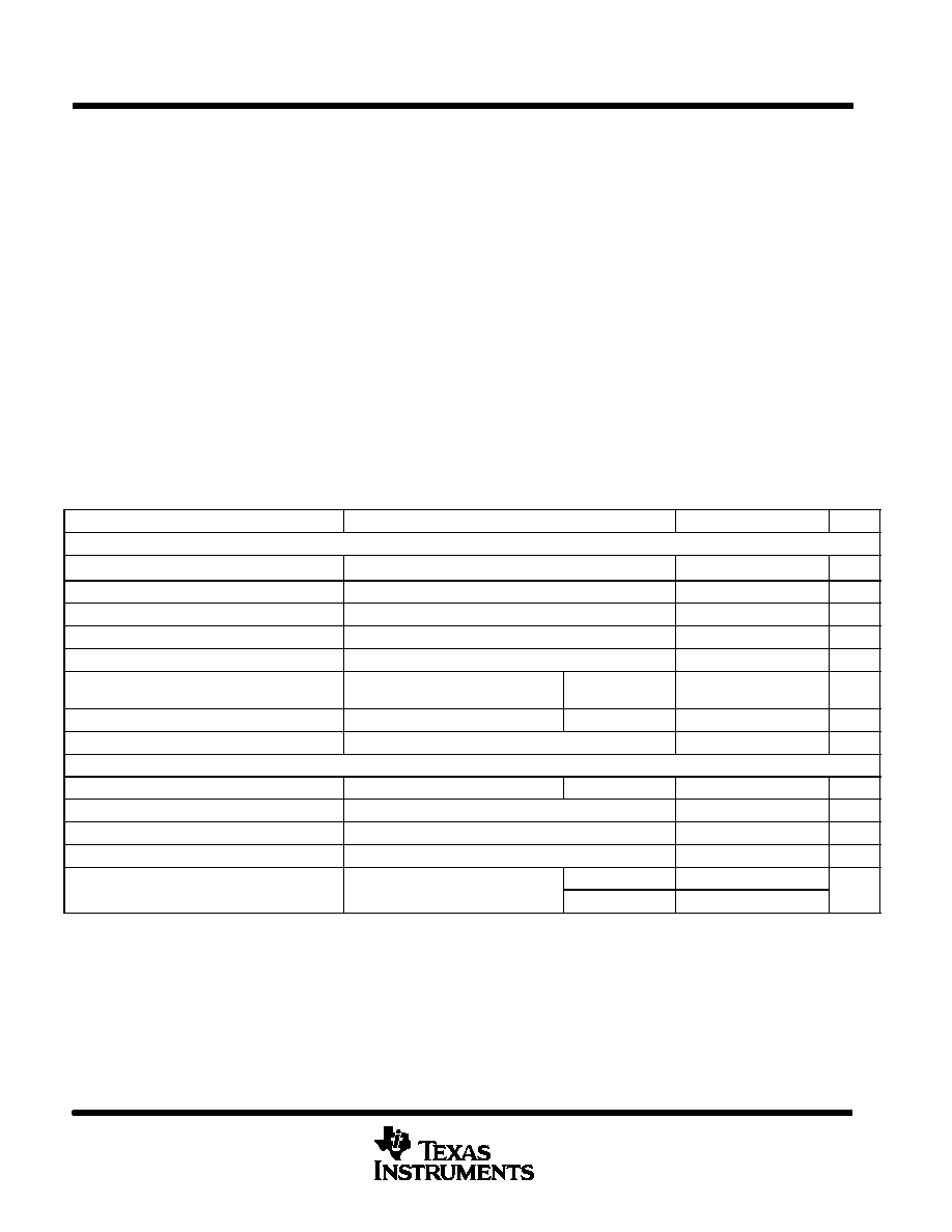
electrical characteristics, TA = –40_C to 125_C, VCC = 15 V (see Note 1), RT = 10 k, CT = 3.3 nF, and
TA = TJ (unless otherwise stated)
PARAMETER
TEST CONDITIONS
MIN
TYP
MAX
UNITS
Reference Section
Output voltage
TJ = 25_C,
IO = 1 mA
4.95
5.0
5.05
V
Line regulation voltage
VIN = 12 V to 25 V
6
20
mV
Load regulation voltage
IO = 1 mA to 20 mA
6
25
mV
Temperature stability
See Notes 2 and 3
0.2
0.4
mV/
_C
Total output variation voltage
Line, Load, Temp.
4.9
5.1
V
Output noise voltage
f = 10 Hz to 10 kHz,
See Note 2
TJ = 25_C
50
V
Long term stability
1000 hours,
See Note 2
TA = 125_C
5
25
mV
Output short-circuit current
–30
–100
–180
mA
Oscillator Section
Initial accuracy
See Note 4
TJ = 25_C
47
52
57
kHz
Voltage stability
VCC = 12 V to 25 V
0.2
1
%
Temperature stability
TA = MIN to MAX, See Note 2
5
%
Amplitude peak-to-peak
V pin 7,
See Note 2
1.7
V
Discharge current
V pin 7
2 V
See Note 5
TJ = 25_C
7.8
8.3
8.8
mA
Discharge current
V pin 7 = 2 V,
See Note 5
TJ = Full range
7.5
8.8
mA
相關(guān)PDF資料 |
PDF描述 |
|---|---|
| UC3827Q-1 | 1 A SWITCHING CONTROLLER, 500 kHz SWITCHING FREQ-MAX, PQCC28 |
| UC3842ADX | |
| UC3843ADX | |
| UC3843ADW | 1 A SWITCHING CONTROLLER, 500 kHz SWITCHING FREQ-MAX, PDSO16 |
| UC3843D1X | |
相關(guān)代理商/技術(shù)參數(shù) |
參數(shù)描述 |
|---|---|
| UC2843AQD8RG4Q1 | 功能描述:電流型 PWM 控制器 Auto Cat Current- Mode PWM Controller RoHS:否 制造商:Texas Instruments 開關(guān)頻率:27 KHz 上升時間: 下降時間: 工作電源電壓:6 V to 15 V 工作電源電流:1.5 mA 輸出端數(shù)量:1 最大工作溫度:+ 105 C 安裝風(fēng)格:SMD/SMT 封裝 / 箱體:TSSOP-14 |
| UC2843AQD8RQ1 | 功能描述:電流型 PWM 控制器 Auto Cat Crnt-Mode PWM Controller RoHS:否 制造商:Texas Instruments 開關(guān)頻率:27 KHz 上升時間: 下降時間: 工作電源電壓:6 V to 15 V 工作電源電流:1.5 mA 輸出端數(shù)量:1 最大工作溫度:+ 105 C 安裝風(fēng)格:SMD/SMT 封裝 / 箱體:TSSOP-14 |
| UC2843AQDR | 功能描述:電流型 PWM 控制器 Auto Cat Crrnt-Mode RoHS:否 制造商:Texas Instruments 開關(guān)頻率:27 KHz 上升時間: 下降時間: 工作電源電壓:6 V to 15 V 工作電源電流:1.5 mA 輸出端數(shù)量:1 最大工作溫度:+ 105 C 安裝風(fēng)格:SMD/SMT 封裝 / 箱體:TSSOP-14 |
| UC2843AQDRHT | 制造商:Rochester Electronics LLC 功能描述:- Tape and Reel |
| UC2843AQG3 | 功能描述:電流型 PWM 控制器 Current Mode PWM RoHS:否 制造商:Texas Instruments 開關(guān)頻率:27 KHz 上升時間: 下降時間: 工作電源電壓:6 V to 15 V 工作電源電流:1.5 mA 輸出端數(shù)量:1 最大工作溫度:+ 105 C 安裝風(fēng)格:SMD/SMT 封裝 / 箱體:TSSOP-14 |
發(fā)布緊急采購,3分鐘左右您將得到回復(fù)。