- 您現(xiàn)在的位置:買賣IC網(wǎng) > PDF目錄98306 > TVP5154APNPR (TEXAS INSTRUMENTS INC) COLOR SIGNAL DECODER, PQFP128 PDF資料下載
參數(shù)資料
| 型號: | TVP5154APNPR |
| 廠商: | TEXAS INSTRUMENTS INC |
| 元件分類: | 顏色信號轉(zhuǎn)換 |
| 英文描述: | COLOR SIGNAL DECODER, PQFP128 |
| 封裝: | GREEN, PLASTIC, HTQFP-128 |
| 文件頁數(shù): | 78/92頁 |
| 文件大小: | 1089K |
| 代理商: | TVP5154APNPR |
第1頁第2頁第3頁第4頁第5頁第6頁第7頁第8頁第9頁第10頁第11頁第12頁第13頁第14頁第15頁第16頁第17頁第18頁第19頁第20頁第21頁第22頁第23頁第24頁第25頁第26頁第27頁第28頁第29頁第30頁第31頁第32頁第33頁第34頁第35頁第36頁第37頁第38頁第39頁第40頁第41頁第42頁第43頁第44頁第45頁第46頁第47頁第48頁第49頁第50頁第51頁第52頁第53頁第54頁第55頁第56頁第57頁第58頁第59頁第60頁第61頁第62頁第63頁第64頁第65頁第66頁第67頁第68頁第69頁第70頁第71頁第72頁第73頁第74頁第75頁第76頁第77頁當(dāng)前第78頁第79頁第80頁第81頁第82頁第83頁第84頁第85頁第86頁第87頁第88頁第89頁第90頁第91頁第92頁
SLES214C – DECEMBER 2007 – REVISED SEPTEMBER 2010
www.ti.com
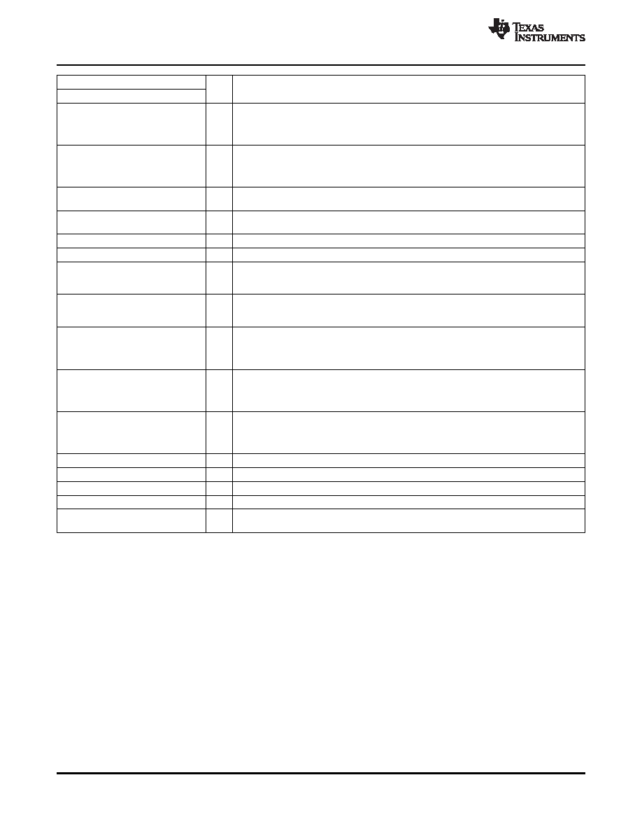
TERMINAL
I/O
DESCRIPTION
NAME
NO.
HSYNC1
100
HSYNC2
77
O
Horizontal synchronization
HSYNC3
58
HSYNC4
39
VSYNC1/PALI1
95
1.
VSYNC: Vertical synchronization
VSYNC2/PALI2
76
O
2.
PALI: PAL line indicator or horizontal lock indicator. For the PAL line indicator, a 1
VSYNC3/PALI3
57
indicates a noninverted line, and a 0 indicates an inverted line.
VSYNC4/PALI4
38
Power down (active low). A 0 on this pin puts the decoder in standby mode. PDN preserves
PDN
122
I
the value of the registers.
Active-low reset. RESETB can be used only when PDN = 1. When RESETB is pulled low, it
RESETB
121
I
resets all the registers and restarts the internal microprocessor.
SCL
120
I/O
I2C serial clock (open drain)
SDA
119
I/O
I2C serial data (open drain)
During power-on reset, this pin is sampled along with pin 117 (I2CA1) to determine the I2C
I2CA0
118
I
address the device is configured to. A 10-k
resistor should pull this either high (to IOVDD)
or low to select different I2C device addresses.
During power-on reset, this pin is sampled along with pin 118 (I2CA0) to determine the I2C
I2CA1
117
I
address the device is configured to. A 10-k
resistor should pull this either high (to IOVDD)
or low to select different I2C device addresses.
CLK1
103
CLK2
84
O
Unscaled system data clock at either 27 MHz or 54 MHz
CLK3
61
CLK4
42
SCLK1
104
SCLK2
85
Scaled system data clock at 27 MHz. This signal can be used to qualify scaled/unscaled
O
SCLK3
62
data when the unscaled system data clock is set to 54 MHz.
SCLK4
43
External clock reference. The user may connect XIN to an oscillator or to one terminal of a
XIN/OSC
124
I
crystal oscillator. The user may connect XOUT to the other terminal of the crystal oscillator
XOUT
123
O
or not connect XOUT at all. One single 14.31818-MHz crystal or oscillator is needed for
ITU-R BT.601 sampling, for all supported standards.
CH1_OUT[7:0]
105–112
O
Decoded ITU-R BT.656 output/YCbCr 4:2:2 output with discrete sync for channel 1
CH2_OUT[7:0]
86–93
O
Decoded ITU-R BT.656 output/YCbCr 4:2:2 output with discrete sync for channel 2
CH3_OUT[7:0]
67–74
O
Decoded ITU-R BT.656 output/YCbCr 4:2:2 output with discrete sync for channel 3
CH4_OUT[7:0]
48–55
O
Decoded ITU-R BT.656 output/YCbCr 4:2:2 output with discrete sync for channel 4
Test-mode select. This pin should be connected to digital ground for correct device
TMS
36
I
operation.
8
Device Details
Copyright 2007–2010, Texas Instruments Incorporated
Product Folder Link(s): TVP5154A
相關(guān)PDF資料 |
PDF描述 |
|---|---|
| TVP5154APNP | COLOR SIGNAL DECODER, PQFP128 |
| TVP5154PNPG4 | COLOR SIGNAL DECODER, PQFP128 |
| TVP5154PNPRG4 | COLOR SIGNAL DECODER, PQFP128 |
| TVP5154PNPR | COLOR SIGNAL DECODER, PQFP128 |
| TVP5154PNP | COLOR SIGNAL DECODER, PQFP128 |
相關(guān)代理商/技術(shù)參數(shù) |
參數(shù)描述 |
|---|---|
| TVP5154EVM | 功能描述:視頻 IC 開發(fā)工具 TVP5154 Eval Mod RoHS:否 制造商:Texas Instruments 產(chǎn)品:Evaluation Boards 類型:YPbPr to RGBHV Converters 工具用于評估:LMH1251 工作電源電壓:5 V |
| TVP5154PNP | 功能描述:視頻 IC 4Ch Lo Pwr PAL/NTSC/ SECAM Video Decoder RoHS:否 制造商:Fairchild Semiconductor 工作電源電壓:5 V 電源電流:80 mA 最大工作溫度:+ 85 C 封裝 / 箱體:TSSOP-28 封裝:Reel |
| TVP5154PNP | 制造商:Texas Instruments 功能描述:4-Channel Video Decoder |
| TVP5154PNPG4 | 制造商:TI 制造商全稱:Texas Instruments 功能描述:4-CHANNEL LOW-POWER PAL/NTSC/SECAM VIDEO DECODER WITH INDEPENDENT SCALERS AND FAST LOCK |
| TVP5154PNPR | 功能描述:視頻 IC 4Ch Lo Pwr PAL/NTSC SECAM Video Decoder RoHS:否 制造商:Fairchild Semiconductor 工作電源電壓:5 V 電源電流:80 mA 最大工作溫度:+ 85 C 封裝 / 箱體:TSSOP-28 封裝:Reel |
發(fā)布緊急采購,3分鐘左右您將得到回復(fù)。