- 您現(xiàn)在的位置:買賣IC網(wǎng) > PDF目錄98306 > TVP5151IPBSQ1 (TEXAS INSTRUMENTS INC) COLOR SIGNAL DECODER, PQFP32 PDF資料下載
參數(shù)資料
| 型號: | TVP5151IPBSQ1 |
| 廠商: | TEXAS INSTRUMENTS INC |
| 元件分類: | 顏色信號轉(zhuǎn)換 |
| 英文描述: | COLOR SIGNAL DECODER, PQFP32 |
| 封裝: | GREEN, PLASTIC, QFP-32 |
| 文件頁數(shù): | 78/86頁 |
| 文件大小: | 964K |
| 代理商: | TVP5151IPBSQ1 |
第1頁第2頁第3頁第4頁第5頁第6頁第7頁第8頁第9頁第10頁第11頁第12頁第13頁第14頁第15頁第16頁第17頁第18頁第19頁第20頁第21頁第22頁第23頁第24頁第25頁第26頁第27頁第28頁第29頁第30頁第31頁第32頁第33頁第34頁第35頁第36頁第37頁第38頁第39頁第40頁第41頁第42頁第43頁第44頁第45頁第46頁第47頁第48頁第49頁第50頁第51頁第52頁第53頁第54頁第55頁第56頁第57頁第58頁第59頁第60頁第61頁第62頁第63頁第64頁第65頁第66頁第67頁第68頁第69頁第70頁第71頁第72頁第73頁第74頁第75頁第76頁第77頁當(dāng)前第78頁第79頁第80頁第81頁第82頁第83頁第84頁第85頁第86頁
TVP5151
SLES241C – SEPTEMBER 2009 – REVISED SEPTEMBER 2010
www.ti.com
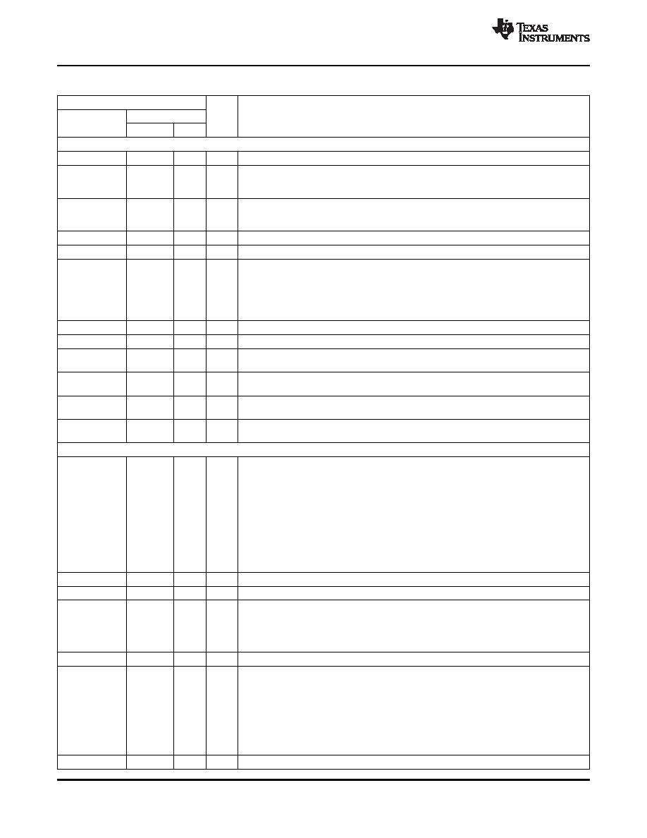
Table 2-1. Terminal Functions
TERMINAL
NO.
I/O
DESCRIPTION
NAME
ZQC
PBS
Analog Section
AGND
E1
7
G
Substrate. Connect to analog ground.
Analog input. Connect to the video analog input via 0.1-F capacitor. The maximum input
AIP1A
A1
1
I
range is 0-0.75 VPP, and may require an attenuator to reduce the input amplitude to the
desired level. If not used, connect to AGND via a 0.1-F capacitor (see Figure 6-1).
Analog input. Connect to the video analog input via 0.1-F capacitor. The maximum input
AIP1B
B1
2
I
range is 0-0.75 VPP, and may require an attenuator to reduce the input amplitude to the
desired level. If not used, connect to AGND via a 0.1-F capacitor (see Figure 6-1).
CH_AGND
A3
31
G
Analog ground
CH_AVDD
A2
32
P
Analog supply. Connect to 1.8-V analog supply.
B2, B3,
B6, C4,
C5,
NC
–
No connect
D3–D6,
E2–E5,
F2, F5, F6
PLL_AGND
C2
3
G
PLL ground. Connect to analog ground.
PLL_AVDD
C1
4
P
PLL supply. Connect to 1.8-V analog supply.
A/D reference negative output. Connect to analog ground through a 1-F capacitor. Also, it
REFM
A4
30
O
is recommended to connect directly to REFP through a 1-F capacitor (see Figure 6-1).
A/D reference positive output. Connect to analog ground through a 1-F capacitor (see
REFP
B4
29
O
External clock reference input. Connect to analog ground if an external single-ended
XTAL1/OSC
D2
5
I
oscillator is connected to AVID/CLK_IN pin.
External clock reference output. Not connected if XTAL1 or CLK_IN is driven by an external
XTAL2
D1
6
O
single-ended oscillator.
Digital Section
Active video indicator output/external clk input
When XTAL1 is used as a reference clock and this terminal is left unconnected, this
terminal is internally pulled down.
When XTAL1 is used as a reference clock and AVID output is required, this pin must be
AVID/CLK_IN
A6
26
I/O
low until terminal is configured as an output. This may be dependent on external circuitry
connected to this terminal.
When XTAL 1 is connected to ground, CLK_IN may be connected to an external
single-ended oscillator from a 1.8-V to 3.3-V compatible clock signal depending on
IO_DVDD voltage.
DGND
E6
19
G
Digital ground
DVDD
E7
20
P
Digital supply. Connect to 1.8-V digital supply.
FID: Odd/even field indicator or vertical lock indicator. For the odd/even indicator, a 1
indicates the odd field.
FID/GLCO
C6
23
O
GLCO: This serial output carries color PLL information. A slave device can decode the
information to allow chrominance frequency control from the TVP5151 decoder. Data is
transmitted at the SCLK rate in Genlock mode. In RTC mode, SCLK/4 is used.
HSYNC
A7
25
O
Horizontal synchronization signal
INTREQ: Interrupt request output
GPCL/VBLK: General-purpose control logic. This terminal has two functions:
INTREQ/GPCL/
GPCL: General-purpose output. In this mode the state of GPCL is directly programmed
B5
27
O
VBLK
via I2C.
VBLK: Vertical blank output. In this mode the GPCL terminal indicates the vertical
blanking interval of the output video. The beginning and end times of this signal are
programmable via I2C.
IO_DVDD
G2
10
P
Digital output supply, 1.8 V to 3.3 V
8
Device Details
Copyright 2009–2010, Texas Instruments Incorporated
相關(guān)PDF資料 |
PDF描述 |
|---|---|
| TVP5151IPBSRQ1 | COLOR SIGNAL DECODER, PQFP32 |
| TVP5151IPBSR | COLOR SIGNAL DECODER, PQFP32 |
| TVP5151IPBS | COLOR SIGNAL DECODER, PQFP32 |
| TVP5151IZQCR | COLOR SIGNAL DECODER, PBGA48 |
| TVP5151IZQC | COLOR SIGNAL DECODER, PBGA48 |
相關(guān)代理商/技術(shù)參數(shù) |
參數(shù)描述 |
|---|---|
| TVP5151IPBSR | 功能描述:視頻 IC UltraLo-Pwr NTSC/PAL SECAM Vid Dec RoHS:否 制造商:Fairchild Semiconductor 工作電源電壓:5 V 電源電流:80 mA 最大工作溫度:+ 85 C 封裝 / 箱體:TSSOP-28 封裝:Reel |
| TVP5151IZQC | 功能描述:視頻 IC UltraLo-Pwr NTSC/PAL SECAM Vid Dec RoHS:否 制造商:Fairchild Semiconductor 工作電源電壓:5 V 電源電流:80 mA 最大工作溫度:+ 85 C 封裝 / 箱體:TSSOP-28 封裝:Reel |
| TVP5151IZQCR | 功能描述:視頻 IC UltraLo-Pwr NTSC/PAL SECAM Vid Dec RoHS:否 制造商:Fairchild Semiconductor 工作電源電壓:5 V 電源電流:80 mA 最大工作溫度:+ 85 C 封裝 / 箱體:TSSOP-28 封裝:Reel |
| TVP5151PBS | 功能描述:視頻 IC UltraLo-Pwr NTSC/PAL SECAM Vid Dec RoHS:否 制造商:Fairchild Semiconductor 工作電源電壓:5 V 電源電流:80 mA 最大工作溫度:+ 85 C 封裝 / 箱體:TSSOP-28 封裝:Reel |
| TVP5151PBSR | 功能描述:視頻 IC UltraLo-Pwr NTSC/PAL SECAM Vid Dec RoHS:否 制造商:Fairchild Semiconductor 工作電源電壓:5 V 電源電流:80 mA 最大工作溫度:+ 85 C 封裝 / 箱體:TSSOP-28 封裝:Reel |
發(fā)布緊急采購,3分鐘左右您將得到回復(fù)。