- 您現(xiàn)在的位置:買賣IC網(wǎng) > PDF目錄98305 > TVP5147M1IPFPRQ1 (TEXAS INSTRUMENTS INC) COLOR SIGNAL DECODER, PQFP80 PDF資料下載
參數(shù)資料
| 型號: | TVP5147M1IPFPRQ1 |
| 廠商: | TEXAS INSTRUMENTS INC |
| 元件分類: | 顏色信號轉換 |
| 英文描述: | COLOR SIGNAL DECODER, PQFP80 |
| 封裝: | PLASTIC, HTQFP-80 |
| 文件頁數(shù): | 15/108頁 |
| 文件大小: | 937K |
| 代理商: | TVP5147M1IPFPRQ1 |
第1頁第2頁第3頁第4頁第5頁第6頁第7頁第8頁第9頁第10頁第11頁第12頁第13頁第14頁當前第15頁第16頁第17頁第18頁第19頁第20頁第21頁第22頁第23頁第24頁第25頁第26頁第27頁第28頁第29頁第30頁第31頁第32頁第33頁第34頁第35頁第36頁第37頁第38頁第39頁第40頁第41頁第42頁第43頁第44頁第45頁第46頁第47頁第48頁第49頁第50頁第51頁第52頁第53頁第54頁第55頁第56頁第57頁第58頁第59頁第60頁第61頁第62頁第63頁第64頁第65頁第66頁第67頁第68頁第69頁第70頁第71頁第72頁第73頁第74頁第75頁第76頁第77頁第78頁第79頁第80頁第81頁第82頁第83頁第84頁第85頁第86頁第87頁第88頁第89頁第90頁第91頁第92頁第93頁第94頁第95頁第96頁第97頁第98頁第99頁第100頁第101頁第102頁第103頁第104頁第105頁第106頁第107頁第108頁
SLES140F – JULY 2005 – REVISED DECEMBER 2010
www.ti.com
1.8
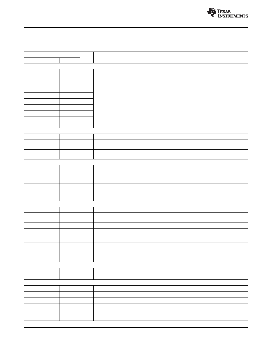
Terminal Functions
Table 1-1. Terminal Functions
TERMINAL
I/O
DESCRIPTION
NAME
NO.
Analog Video
VI_1_A
80
I/O
VI_1_B
1
I
VI_1_A: Analog video input for CVBS/Pb/C or analog video output (see Table 2-79)
VI_1_C
2
I
VI_1_x: Analog video input for CVBS/Pb/C
VI_2_x: Analog video input for CVBS/Y
VI_2_A
7
I
VI_3_x: Analog video input for CVBS/Pr/C
VI_2_B
8
I
VI_4_A: Analog video input for CVBS/Y
Up to ten composite, four S-video, and two composite or three component video inputs (or a
VI_2_C
9
I
combination thereof) can be supported.
VI_3_A
16
I
The inputs must be ac-coupled. The recommended coupling capacitor is 0.1 F.
The possible input configurations are listed in the input select register at I2C subaddress 00h
VI_3_B
17
I
(see Table 2-12).
VI_3_C
18
I
VI_4_A
23
I
Clock Signals
DATACLK
40
O
Line-locked data output clock
External clock reference input. It can be connected to an external oscillator with a 1.8-V
XTAL1
74
I
compatible clock signal or a 14.31818-MHz crystal oscillator.
External clock reference output. Not connected if XTAL1 is driven by an external single-ended
XTAL2
75
O
oscillator.
Digital Video
57, 58, 59,
Digital video output of CbCr, C[9] is MSB and C[0] is LSB. C_0 and C_[9-2] can be used as
60, 63, 64,
programmable general purpose I/O. C_1 (pin 69) requires an external pulldown resistor and
C_[9:0]
I/O
65, 66, 69,
should not be used for general purpose I/0.
70
For the 8-bit mode, the two LSBs are ignored. Unused outputs can be left unconnected.
43, 44, 45,
46, 47, 50,
Digital video output of Y/YCbCr, Y[9] is MSB and Y[0] is LSB.
Y[9:0]
O
51, 52, 53,
For the 8-bit mode, the two LSBs are ignored. Unused outputs can be left unconnected.
54
Miscellaneous Signals
GPIO
35
I/O
Programmable general-purpose I/O
Genlock control output (GLCO) uses real time control (RTC) format.
GLCO/I2CA
37
I/O
During reset, this terminal is an input used to program the I2C address LSB.
INTREQ
30
O
Interrupt request
14, 15, 19,
Not connected. These terminals can be connected to power or ground (compatible with
NC
20, 21, 22,
TVP5146 terminals), internally floating.
24, 25
Power down input:
PWDN
33
I
1 = Power down
0 = Normal mode
RESETB
34
I
Reset input, active low (see Section 2.8)
Host Interface
SCL
28
I
I2C clock input
SDA
29
I/O
I2C data bus
Power Supplies
AGND
26
Analog ground. Connect to analog ground.
A18GND_REF
13
Analog 1.8-V return
A18VDD_REF
12
Analog power for reference 1.8 V
CH1_A18GND
79
Analog 1.8-V return
CH2_A18GND
10
CH1_A18VDD
78
Analog power. Connect to 1.8 V.
14
Introduction
Copyright 2005–2010, Texas Instruments Incorporated
Product Folder Link(s): TVP5147M1
相關PDF資料 |
PDF描述 |
|---|---|
| TVP5147M1IPFPQ1 | COLOR SIGNAL DECODER, PQFP80 |
| TVP5147PFPG4 | COLOR SIGNAL DECODER, PQFP80 |
| TVP5147PFP | COLOR SIGNAL DECODER, PQFP80 |
| TVP5147PFPR | COLOR SIGNAL DECODER, PQFP80 |
| TVP5147PFPRG4 | COLOR SIGNAL DECODER, PQFP80 |
相關代理商/技術參數(shù) |
參數(shù)描述 |
|---|---|
| TVP5147M1PFP | 功能描述:視頻 IC 10B High Qual S-Chip Dig Vid Decoder RoHS:否 制造商:Fairchild Semiconductor 工作電源電壓:5 V 電源電流:80 mA 最大工作溫度:+ 85 C 封裝 / 箱體:TSSOP-28 封裝:Reel |
| TVP5147M1PFP | 制造商:Texas Instruments 功能描述:; Resolution (Bits):10; Supply Current:5 |
| TVP5147M1PFP_07 | 制造商:TI 制造商全稱:Texas Instruments 功能描述:NTSC/PAL/SECAM 2 X 10-Bit Digital Video Decoder With Macrovision Detection, YPbPr Inputs, and 5-Line Comb Filter |
| TVP5147M1PFPG4 | 制造商:TI 制造商全稱:Texas Instruments 功能描述:NTSC/PAL/SECAM 2 X 10-Bit Digital Video Decoder With Macrovision Detection, YPbPr Inputs, and 5-Line Comb Filter |
| TVP5147M1PFPR | 功能描述:視頻 IC 10B Hi Qual Sgl-Chip Dig Vid Dec RoHS:否 制造商:Fairchild Semiconductor 工作電源電壓:5 V 電源電流:80 mA 最大工作溫度:+ 85 C 封裝 / 箱體:TSSOP-28 封裝:Reel |
發(fā)布緊急采購,3分鐘左右您將得到回復。